 |
Theory of Thin-Film Field-Effect Transistors (TFT)(modeling TFT devices)electrical characterization of TFTs |
|
| |
Theory of Thin-Film Field-Effect Transistors (TFT)(modeling TFT devices)electrical characterization of TFTs |
|
These pages describe the
theory behind thin-film transistors. Hope you enjoy it and,
even more, hope it is useful to you. If you want to
reference to this work (and help us get credit for it),
please do so by citing the following papers
Electrical Characterization of Organic Electronic Materials and Devices Peter Stallinga Wiley ISBN:
978-0-470-75009-4
Hardcover
316 pages
|
 |
| Research spends a lot of
effort on optimizing the performance of these devices. We
have contributed to this by studying and modeling the TFT.
What follows is a summary of our research. Probably the most
pressing question is "What is the conduction mechanism?"
(actually this question applies to all organic devices). Is
it hopping conduction or band conduction? Unfortunately, it
is not possible to decide between the two by simple
electrical measurements. Often the 'mobility argument' is
used as a referee. High mobility indicates band conduction
and low mobility points at hopping conduction with 10-6-10-4
cm2/Vs being some sort of division line. However,
we found out that mobilities in a very large range (10-8-1000
cm2/Vs) can be explained without change in
conduction mechanism (Org. Electr. 7, 592 (2006)). In the
following text, we use the nomenclature of band conduction (NV, NC, Eg, etc.),
though we want to point out that it is just giving a name to
the beasts. The only distinction that can be made is
'conductive states' and 'non-conductive states'. One might
mean for instance valence band, but it can equally mean
polarons. The other can be traps, but can equally mean
polarons (!). It is also assumed that the mobility of
conductive states is a fixed value (the 'intrinsic
mobility') and that non-conductive states have zero
mobility. Reality is probably more complicated. We justify
these simplifications by the need to come up with a useful
intuitive model that can easily be understood by a large
community. However, in spite of this, the model that emerges
is remarkably good for explaining actual data. On the other
hand, if you came here for finding an answer to the question
of the conduction model, you came to the wrong place. |
 Polaron; A charge inside it's self-created
lattice distortion. Is it a conductive or non-conductive
state?
|
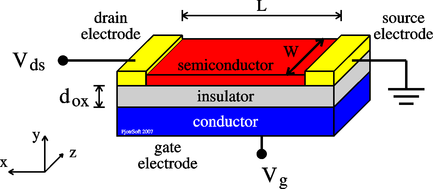 |
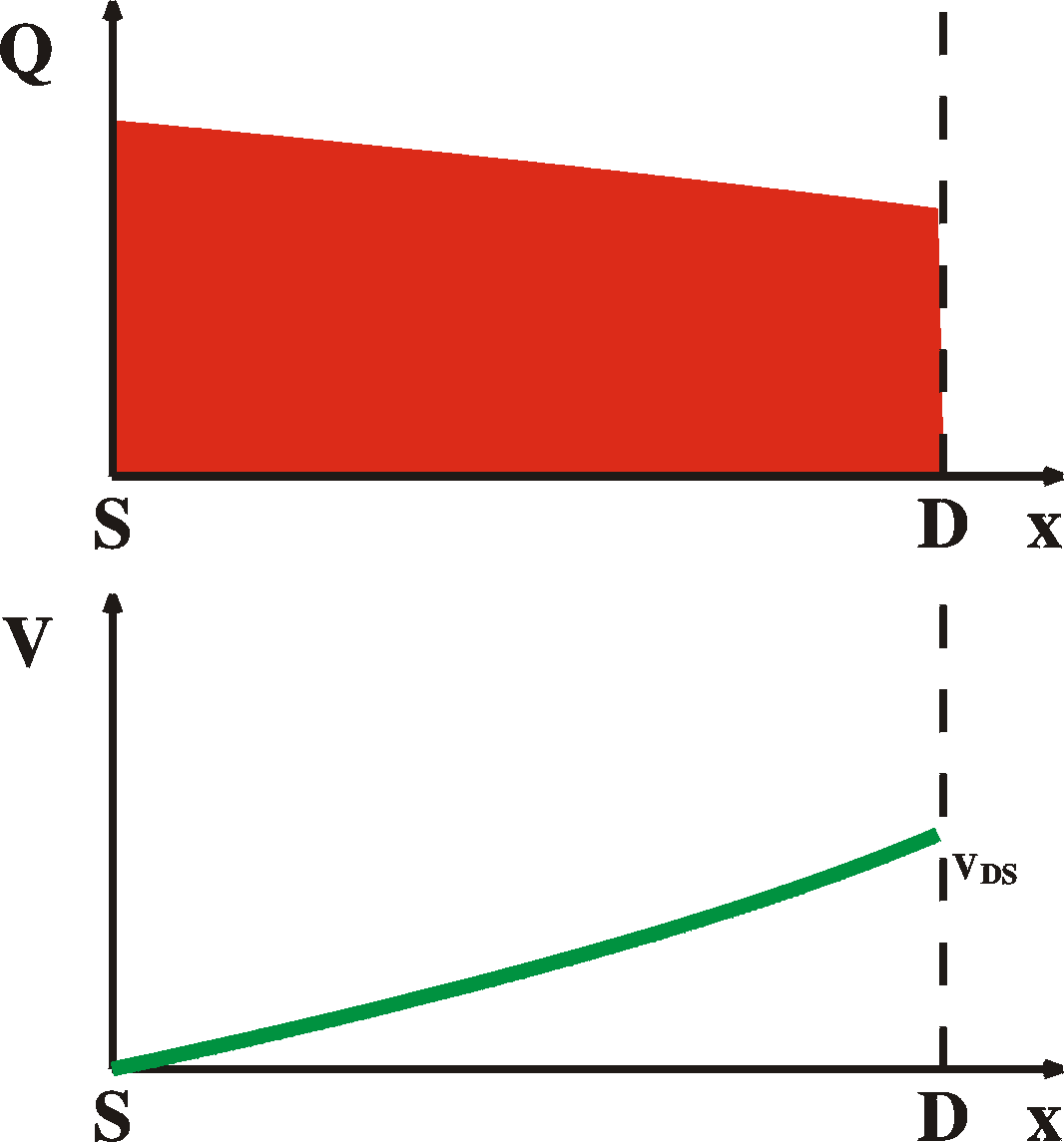
Directions: x: from source to drain y from oxide to surface of film z: along an electrode W: electrode width |
| r(x) = q p(x) = Cox [V(x)-Vg] (1) |
| Ix(x) = -q p(x) m W dV(x)/dx (2) |
|
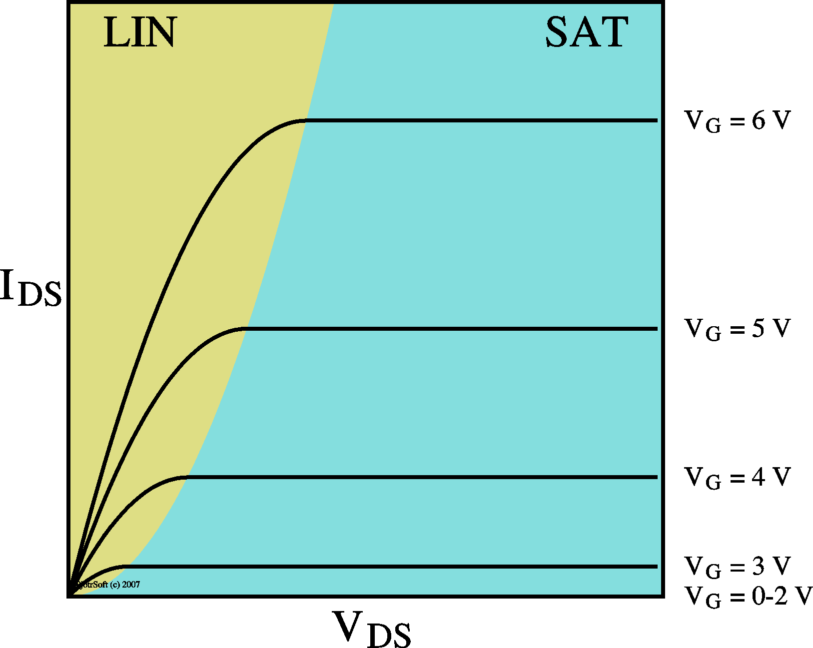
Ids = m Cox [VgVds - Vds2/2] W/L |
 |
 |
 |
 |
 |
 |
|
|
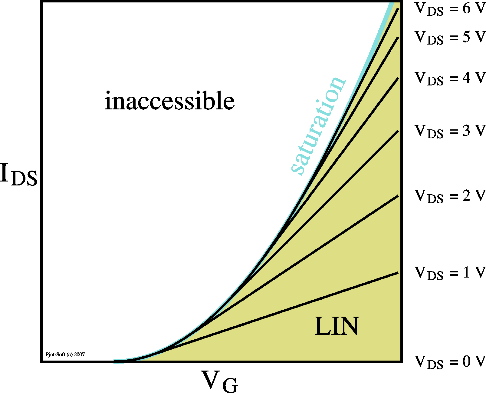
LIN |
onset of SAT |
SAT |
|
Ids = m CoxVgVds W/L |
| mFET |
=
|
|
|
VT = 0 |
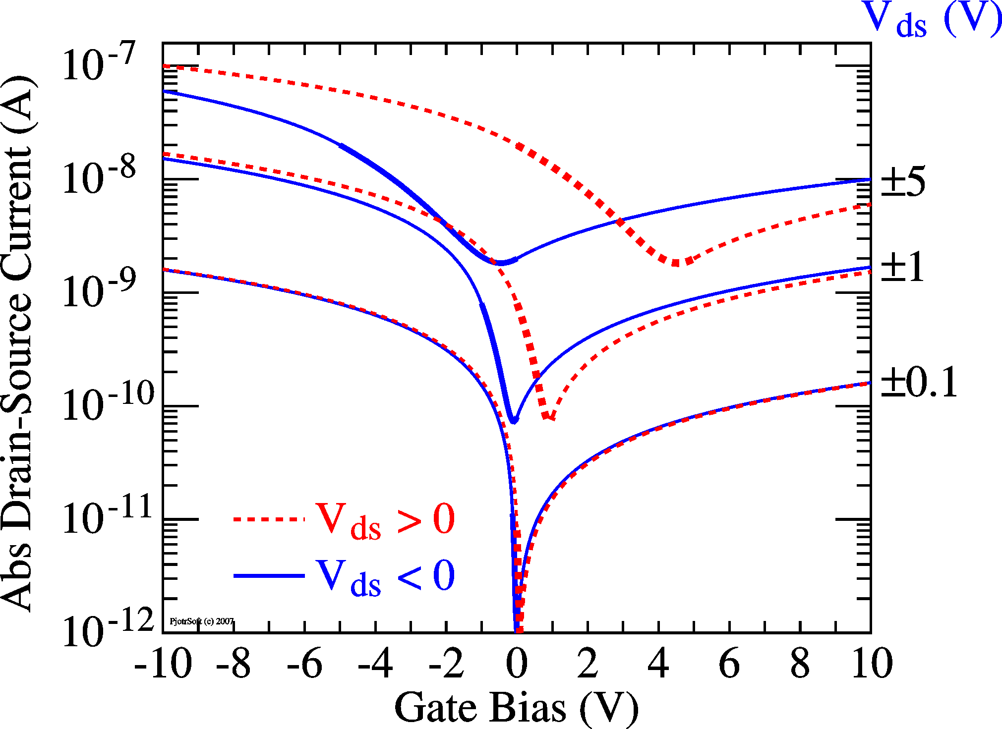
| In many cases, the insulator
is less-than-perfect and currents may exist through the
insulator to the gate. In a very rudimentary way, we can
simulate this by placing a resistor bridging the drain and
the source (assuming the current meter is placed at the
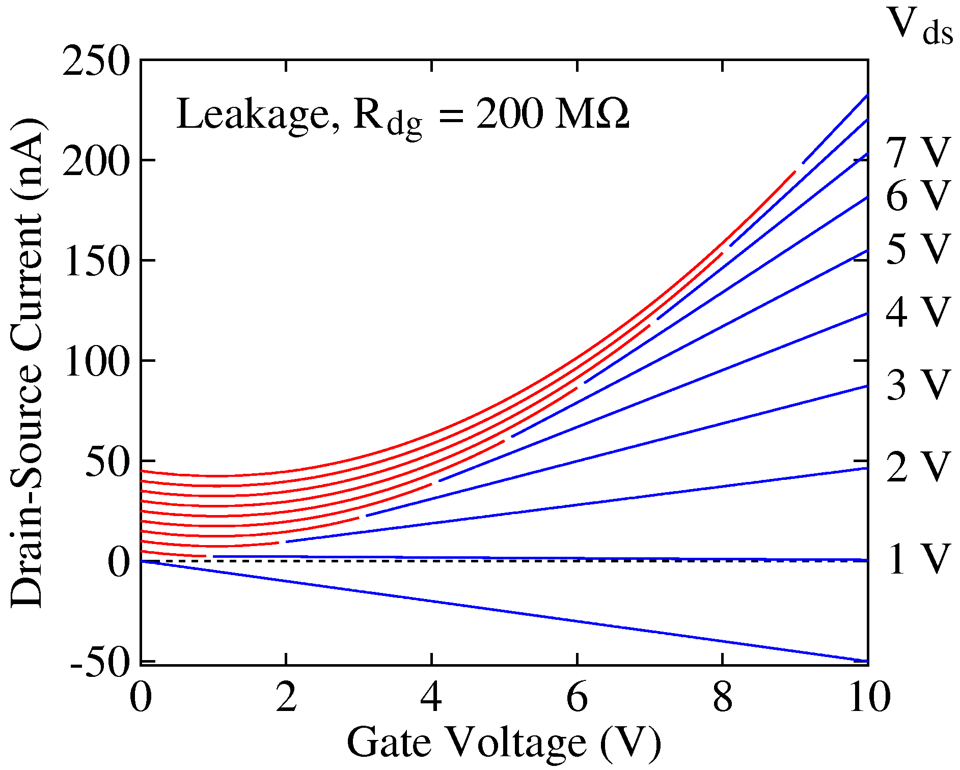
drain), as shown here on the picture on the right. A better simulation would have at every point in space (x) a resistor bridging the channel and the gate, but for the moment these pictures are informative enough, I hope. In the IV curves (left), the curves cross (in the linear region) at Vds = 1/(aRdg), Ids = 1/(2aRdg2)
with a = m Cox W/L
Assuming this simle model of a shunt resistor Rdg, it is easily understood that, to circumnvent measuring the leakage current and focus on the channel current, a good way is to measure the locust curve, (Ids as a function of Vds = Vg). In principle, leakage current should then disappear from the measurements. |
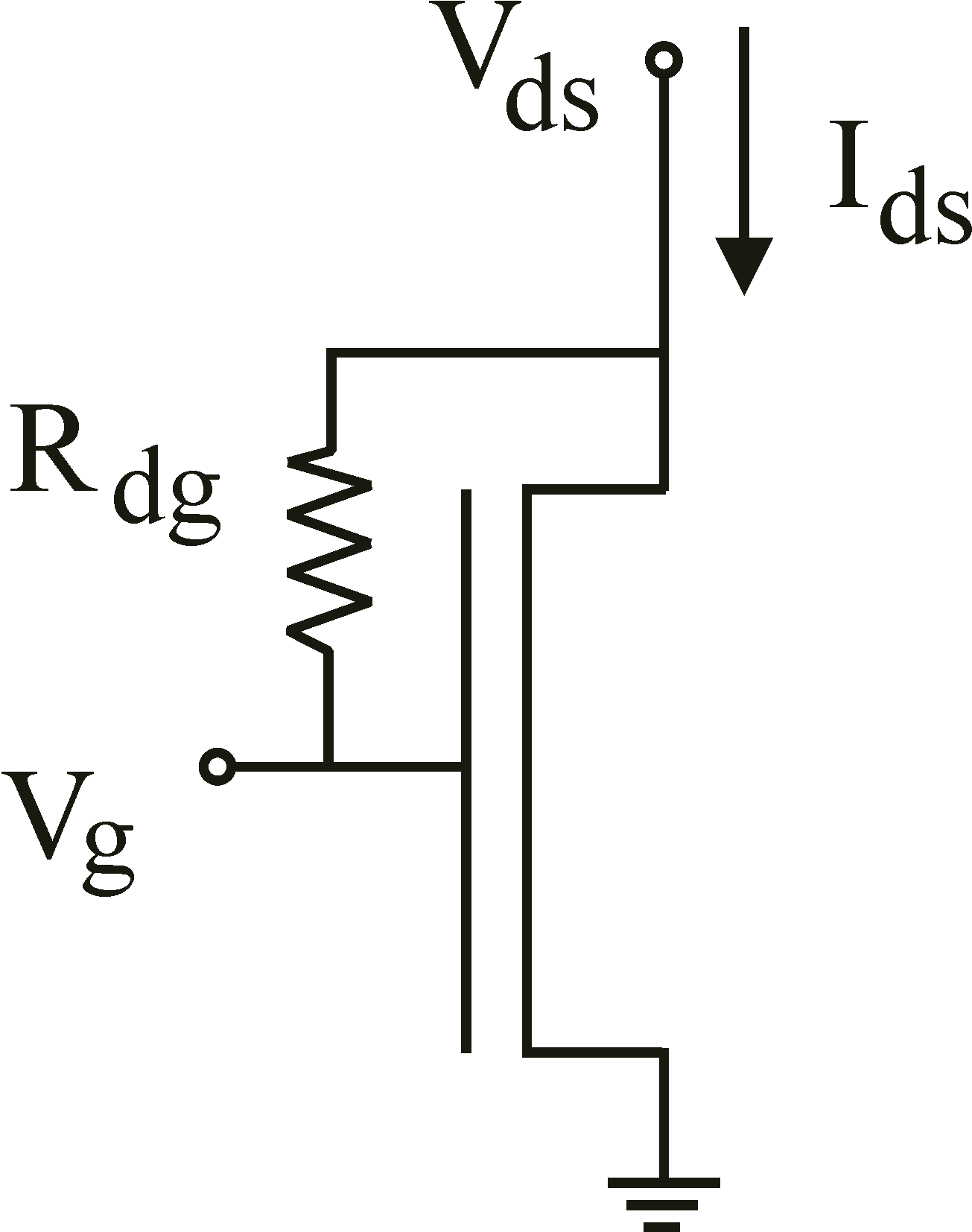 |
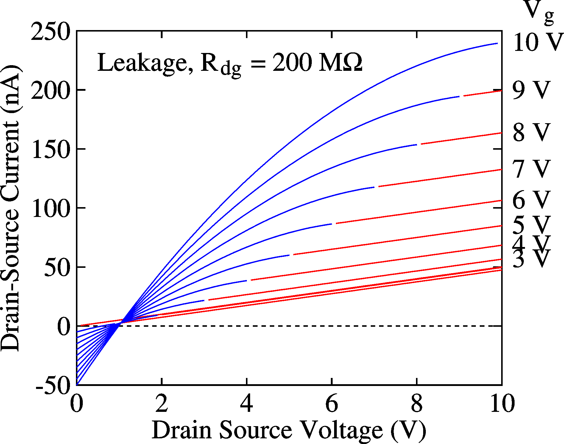 Simulation of leakage current in a TFT (see circuit above). IV curves |
 Simulation of leakage current in a TFT (see circuit above). Transfer curves |
| Ambipolar materials are
materials which have a high electron and hole mobility and
can thus conduct both. Because these electrons and holes can
thus be made to meet somewhere in the middle of the channel,
far away from the electrodes, they can be made to produce
light when they recombine. Such light-emitting field-effect
transistors can also be made from two separate layers, one
with high electron mobility and one with high hole mobility,
but the description here will assume that the material
itself is ambipolar. For such materials, saturation cannot
occur. The reason of this is quite simple. In unipolar
devices, when the density of the holes goes to zero, a large
field can exist while maintaining a small current. At this
point the opposite carrier (n) gets a high density (because n p = ni2
still holds, as long as the currents are low) but because
they have low mobility, they cannot contribute to current.
On the other hand, in ambipolar materials the mobility is
also relatively high and no strong fields can be maintained.
In the equation replacing Eq. 2, Ix(x) = - q [p(x) mp + n(x) mn]
W dV(x)/dx
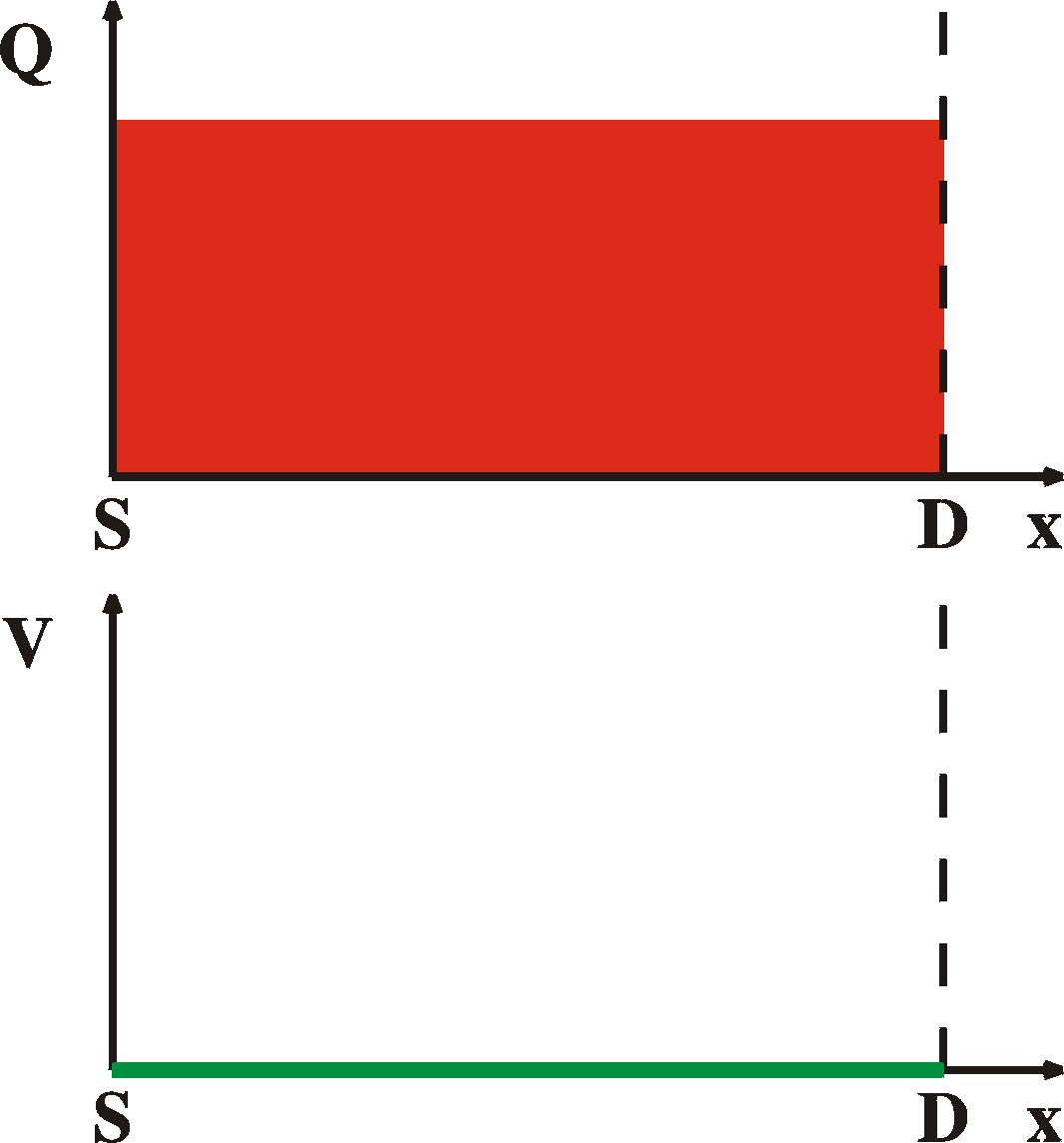
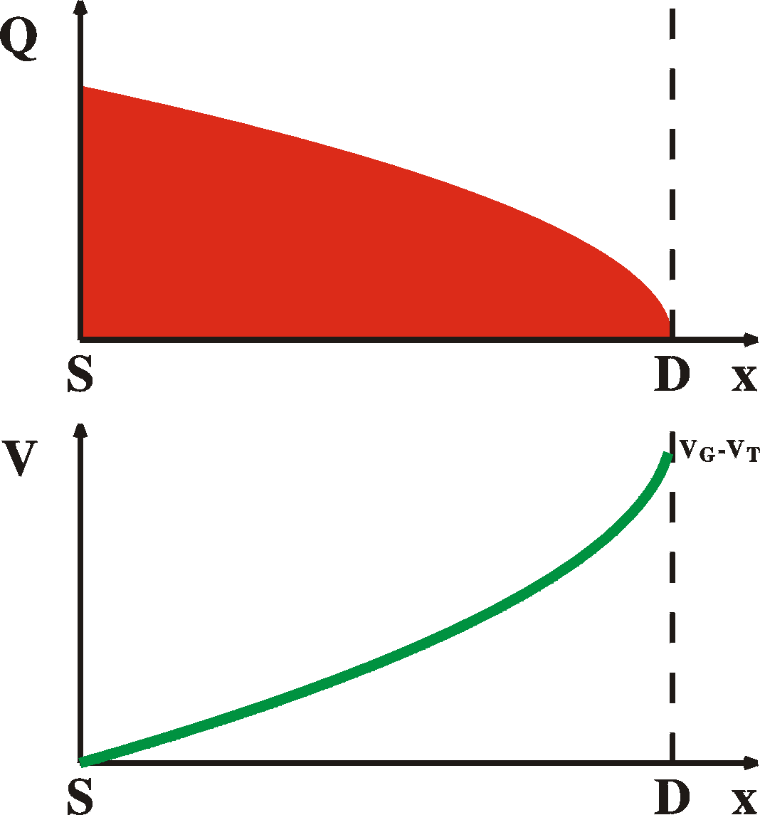
which reduces to the original Equation 2 when mn = 0. It is obvious that always a hole current or an electron current exists. The figure on the left shows an example of the charge and potential distribution in an ambipolar TFT. Note the separate regions of holes and electrons. At the meeting point, electrons and holes can interdiffuse and recombine radiatively. By playing with the gate and drain voltages the position of the cross-over point can be programmed, as well as the total current (and thus light intensity). See Synthetic Metals 156, 1305 (2006) |
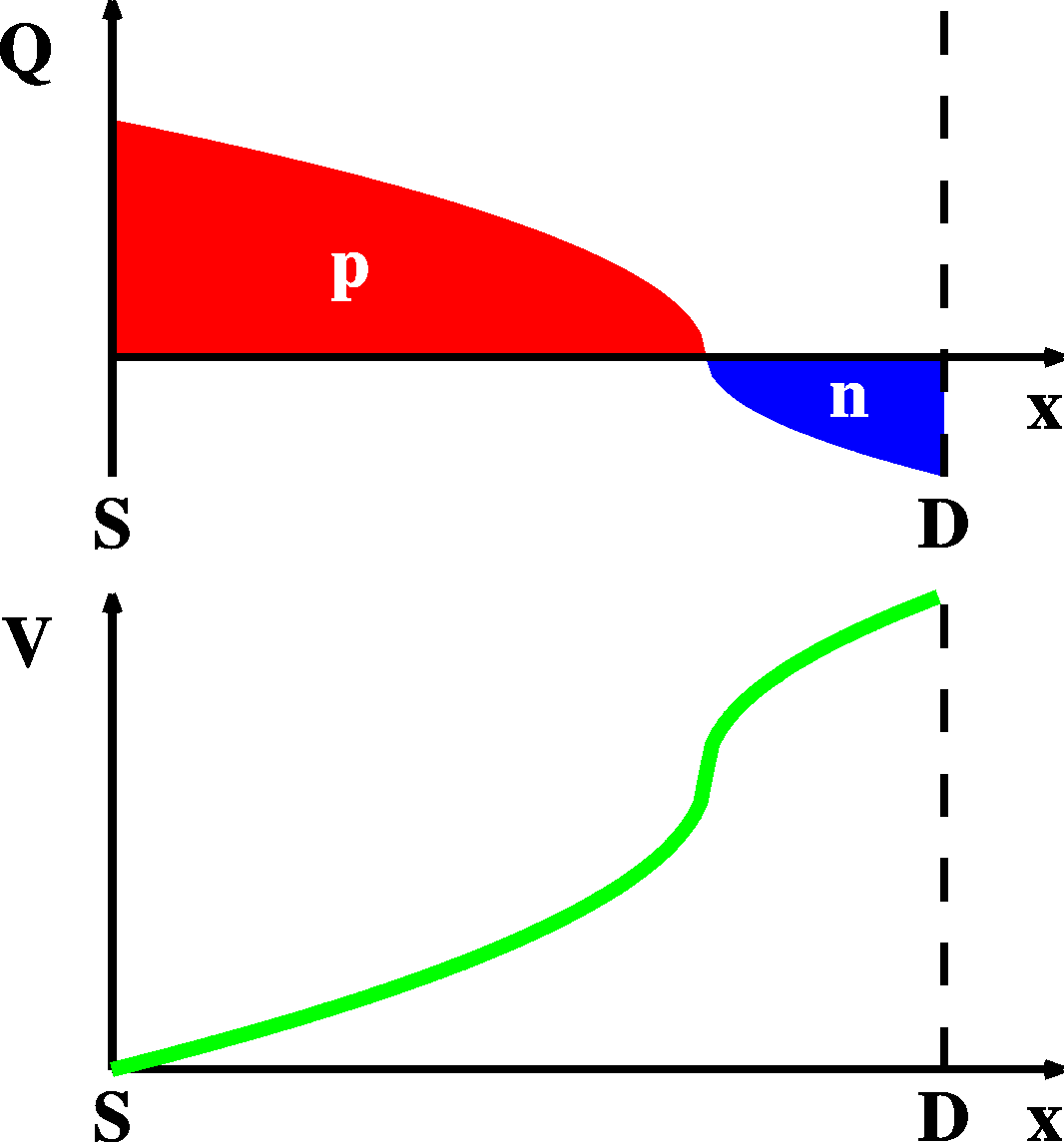 Charge (Q) and potential (V) distribution in an
ambipolar TFT.
|
 |
 |
 |
 |
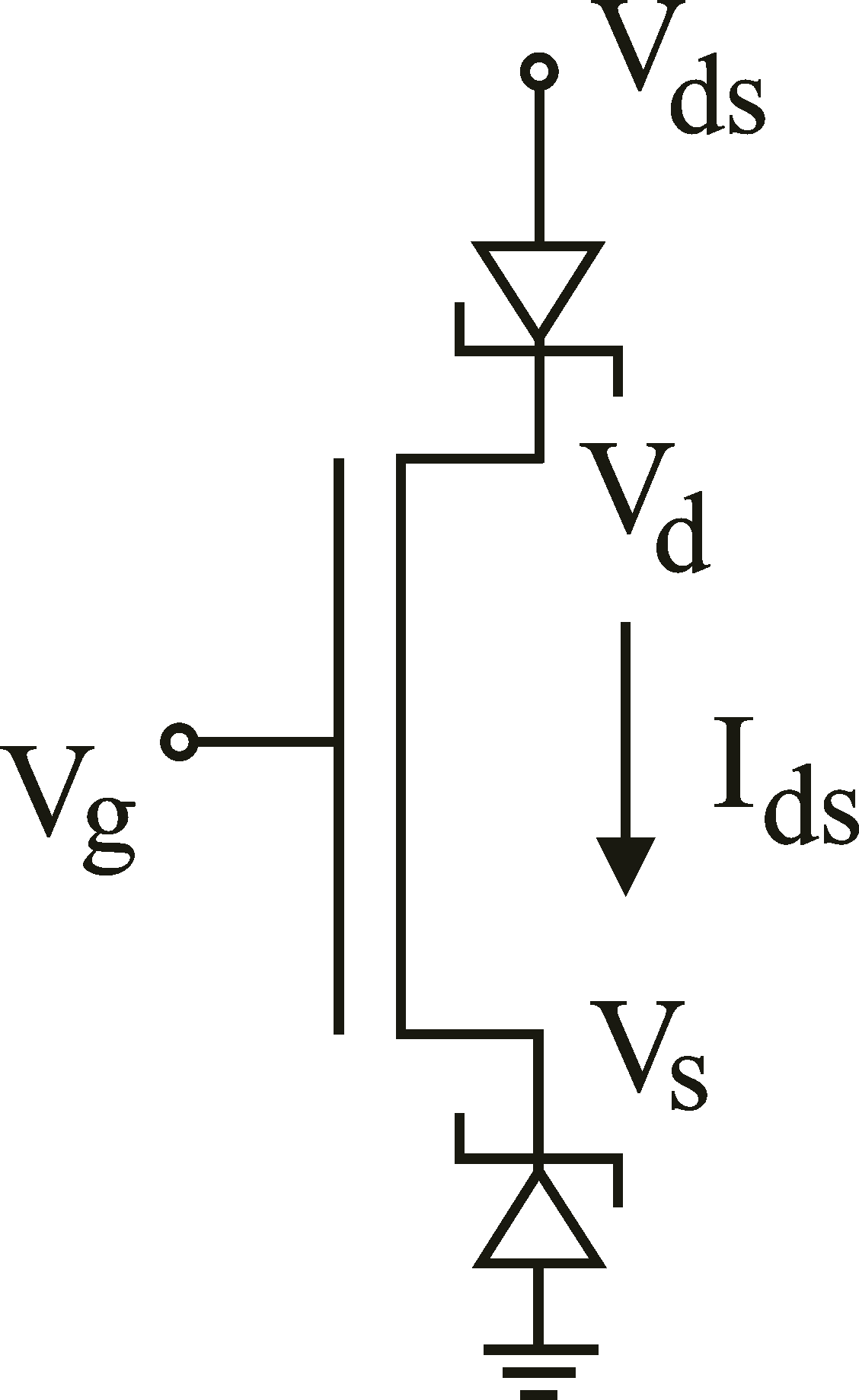
Vs = IdsRc Vd = Vds - Ids Rc Vgs = Vg-Vs Ids = mCox (W/L) Vgs(Vd -Vs ) |
In the above discussion it
was assumed that the injection of carriers is not a limiting
factor. In other words the contacts were considered
low-ohmic However, the contacts can cause a severe barriers
for the injection of carriers. The most obvious one is when
at the electrodes a high-resistive region is formed. This
causes the current to grow sub-linearly in the linear
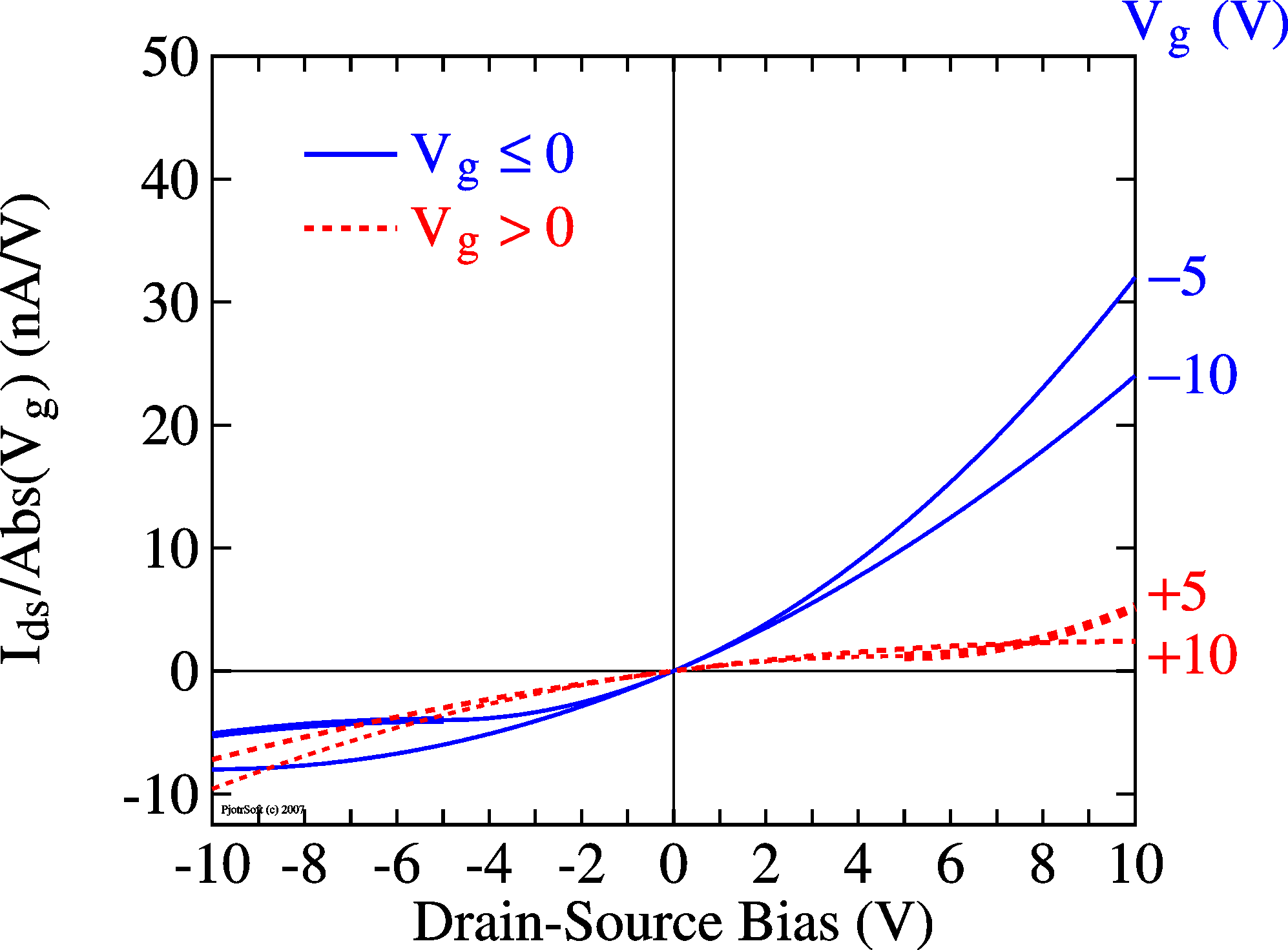
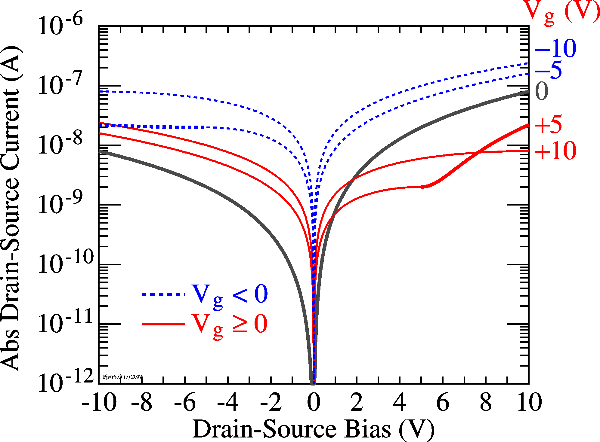
region. This can easily be shown in a simulation. For strong currents, the contact resistance can become the limiting factor and the current saturates and becomes independent of Vg: We have to imagine that the FET is made up of two contact resistances (2Rc) and the channel resistance, connected in series. Initially the current grows linear with VG (as explained by the text above). The channel resistance is thus proportional to 1/Vg.For large Vg the channel resistance disappears and the current settles at Vds / 2Rc. More exact: when the current is increasing, the contact resistance induces a voltage drop at the source, Vs = IdsRc, the field at the source (Vgs) is reduced and the current drops (external observables in bold): |
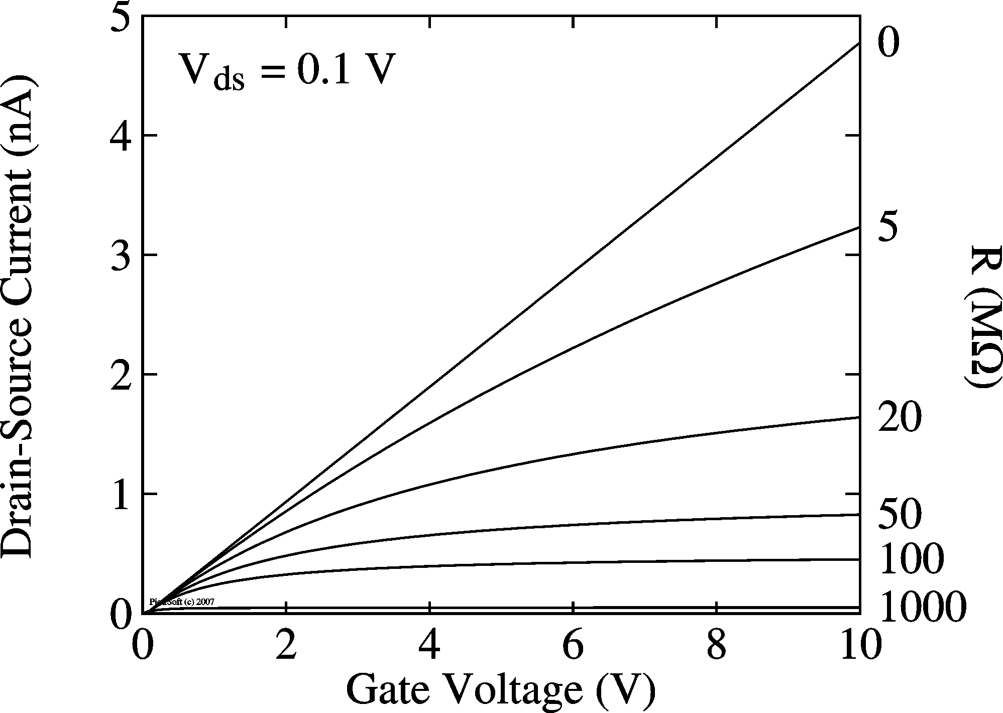 Transfer curves |
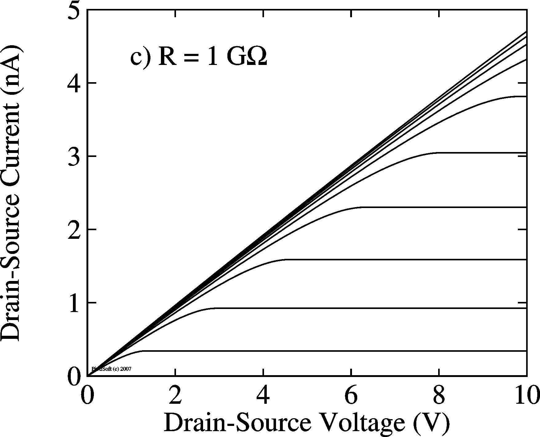 IV Curves |
| The interface regions are not
necessarily ohmic, as described above. Contacts are normally
made of metal and the contact of this metal with a
semiconductor might result in a Schottky diode. When a
depletion layer is formed between the electrodes and the
semiconductor, the current, might be limited by this
Schottky barrier, see the bipolar device
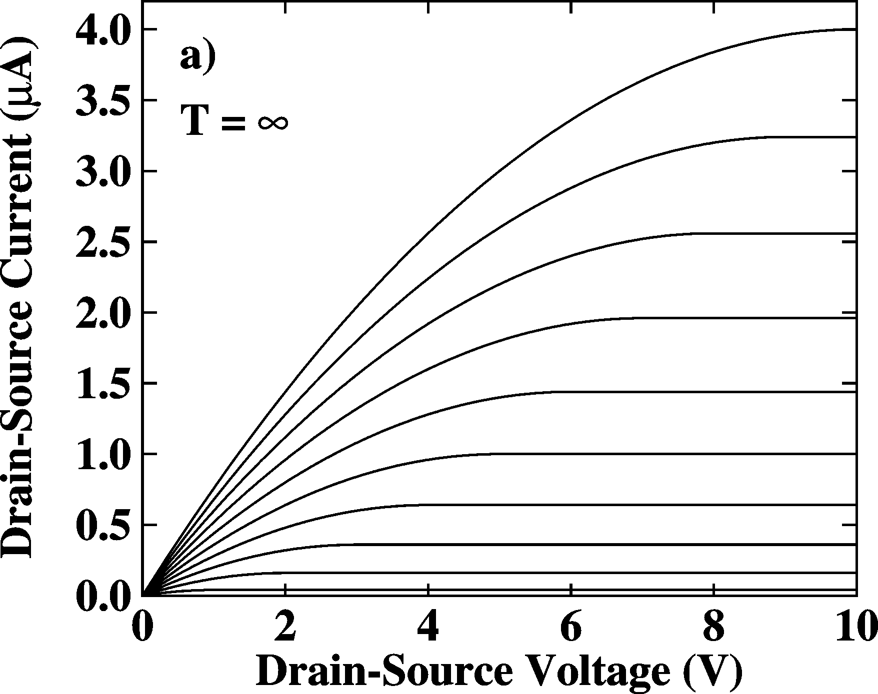
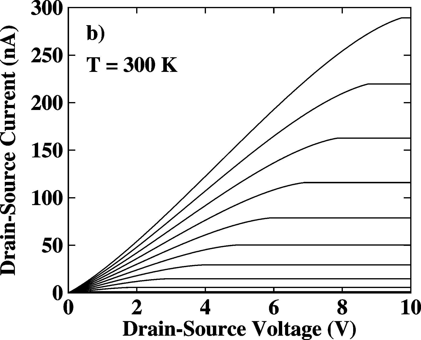
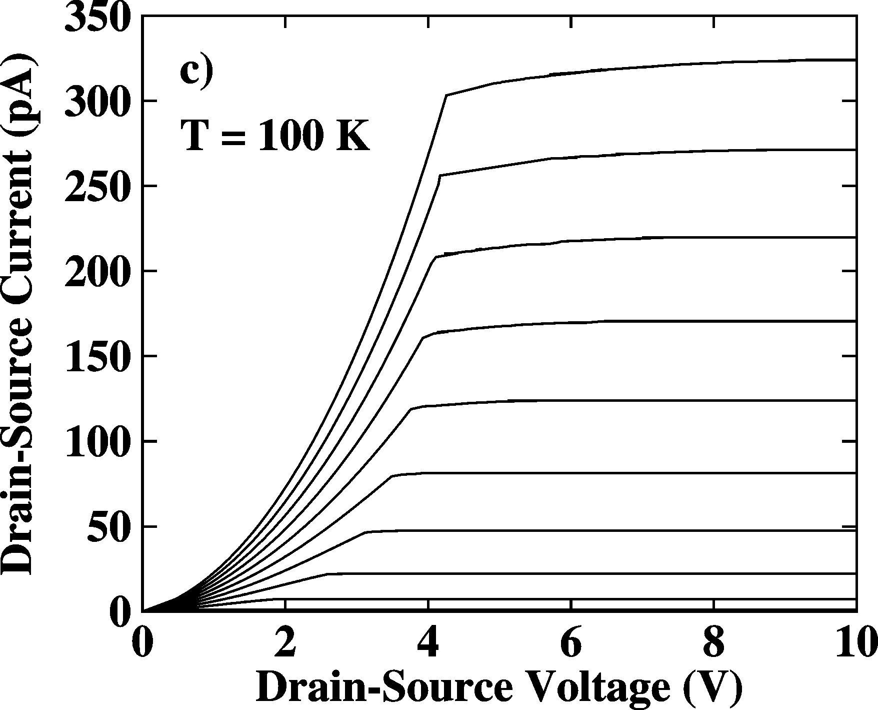
theory pages. When such Schottky barriers exist, they come in pairs, with a forward biased Schottky diode at the drain and a reverse-biased Schottky diode at the source (or vice verse). In other words, the maximum current through the device is a reverse-biased Schottky barrier current. When the Schottky barriers are the limiting elements, the current thus follows a hyperbolic tangent, Ids = tanh(Vds) and saturates at a voltage of approximately Vsat = kT/q = 26 mV at room temperature, see the simulation below. This is not what is normally observed for TFTs. We conclude therefore that Schottky barriers play no role in TFTs. Synthetic Metals 156, 1305 (2006) |
 Equivalent circuit of an FET with Schottky barriers at the contacts. |
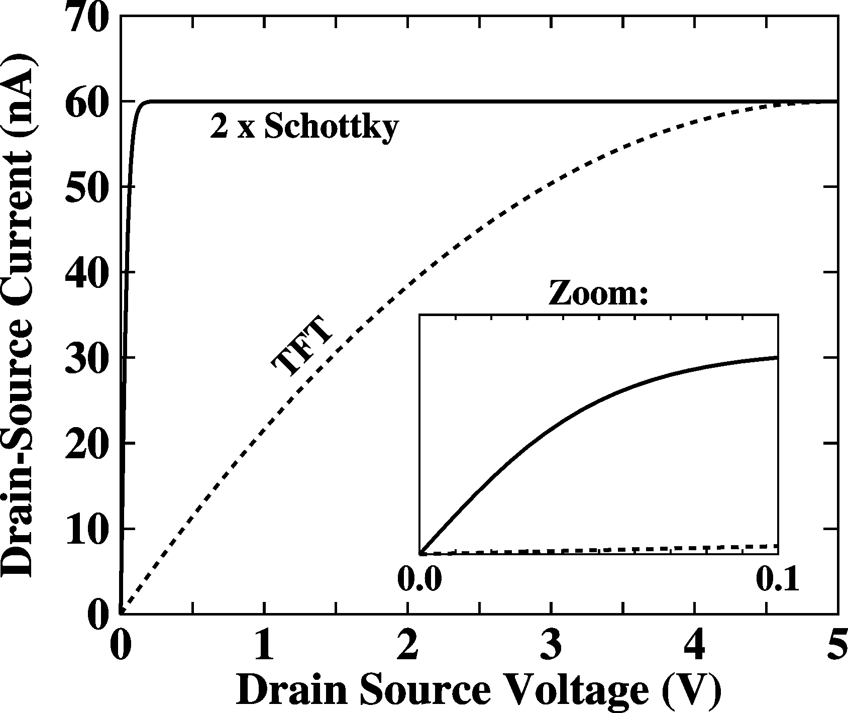 Simulation of an FET with Schottky barriers at the contacts as given on the left. |
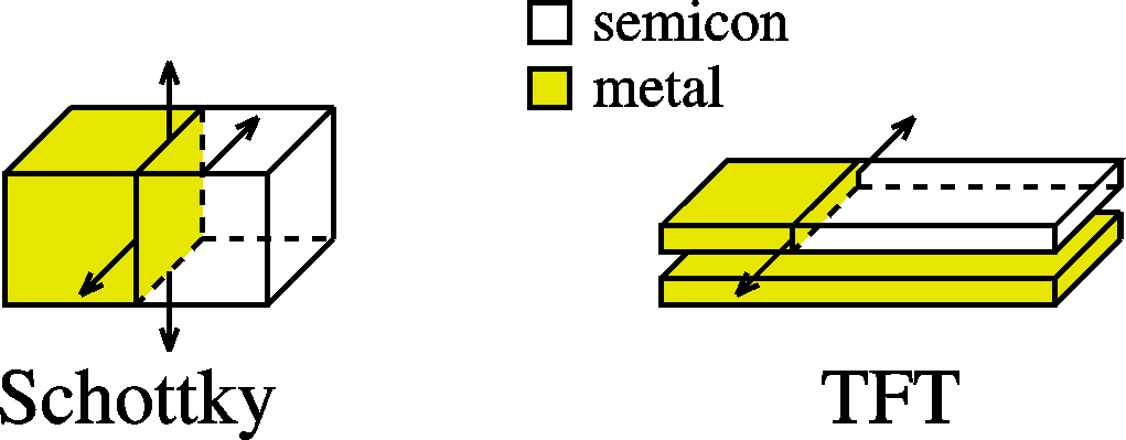
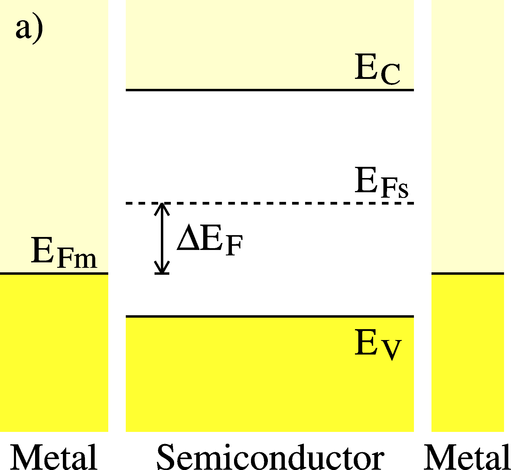 metal-semiconductor-metal TFT system before contact |
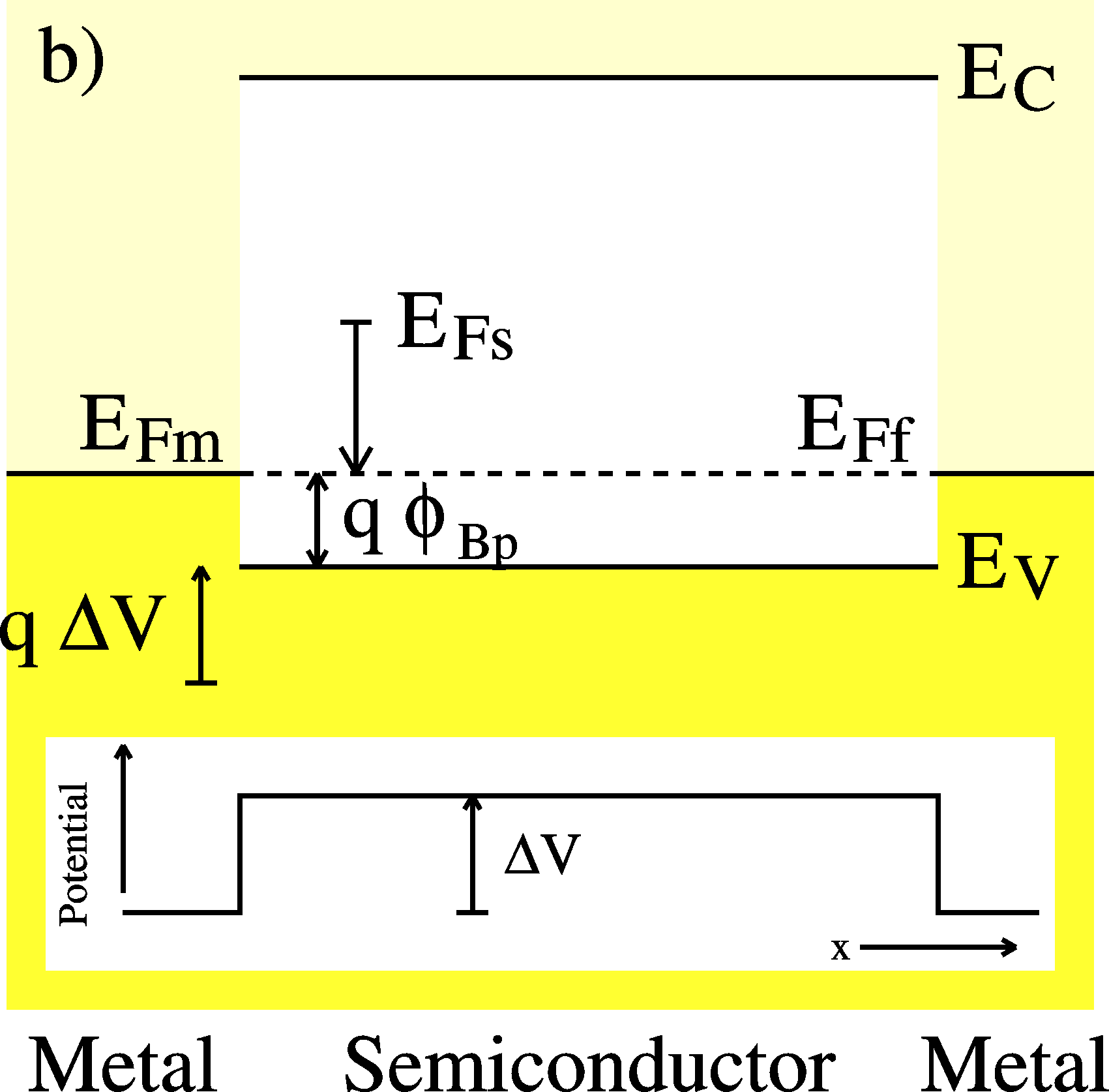 metal-semiconductor-metal TFT system after contact |
 |
 |
 |
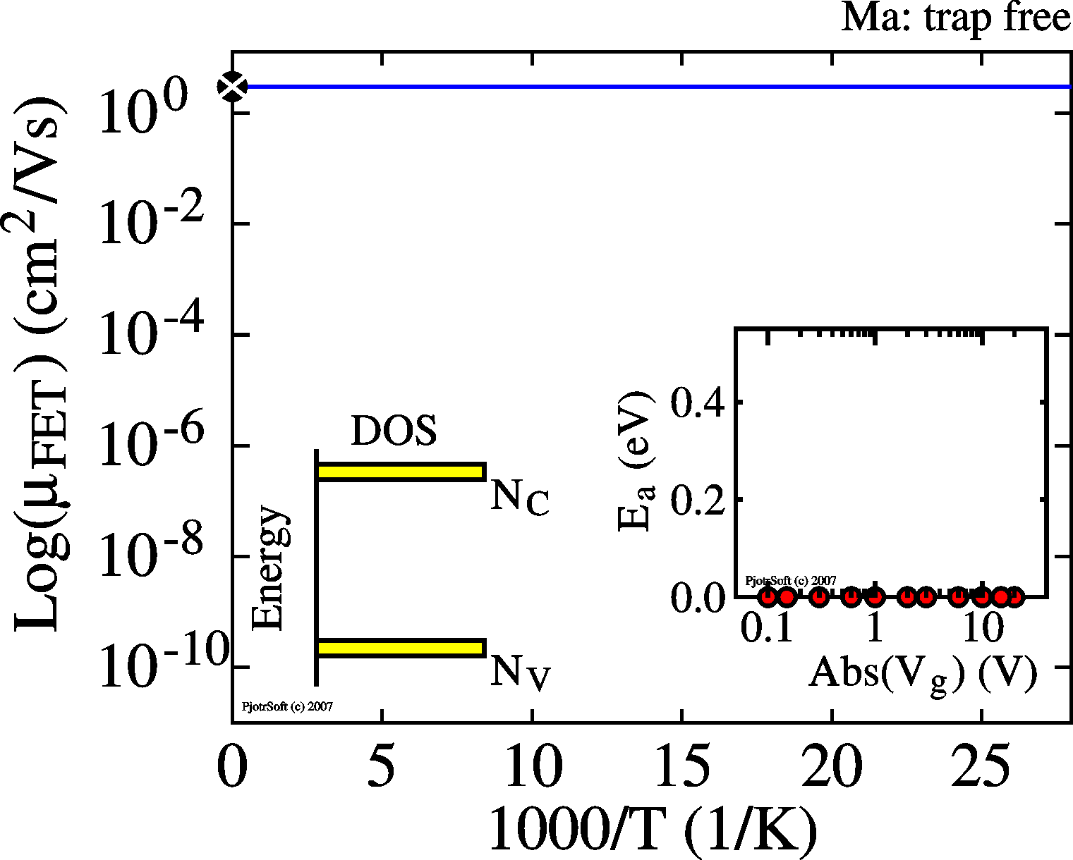 |
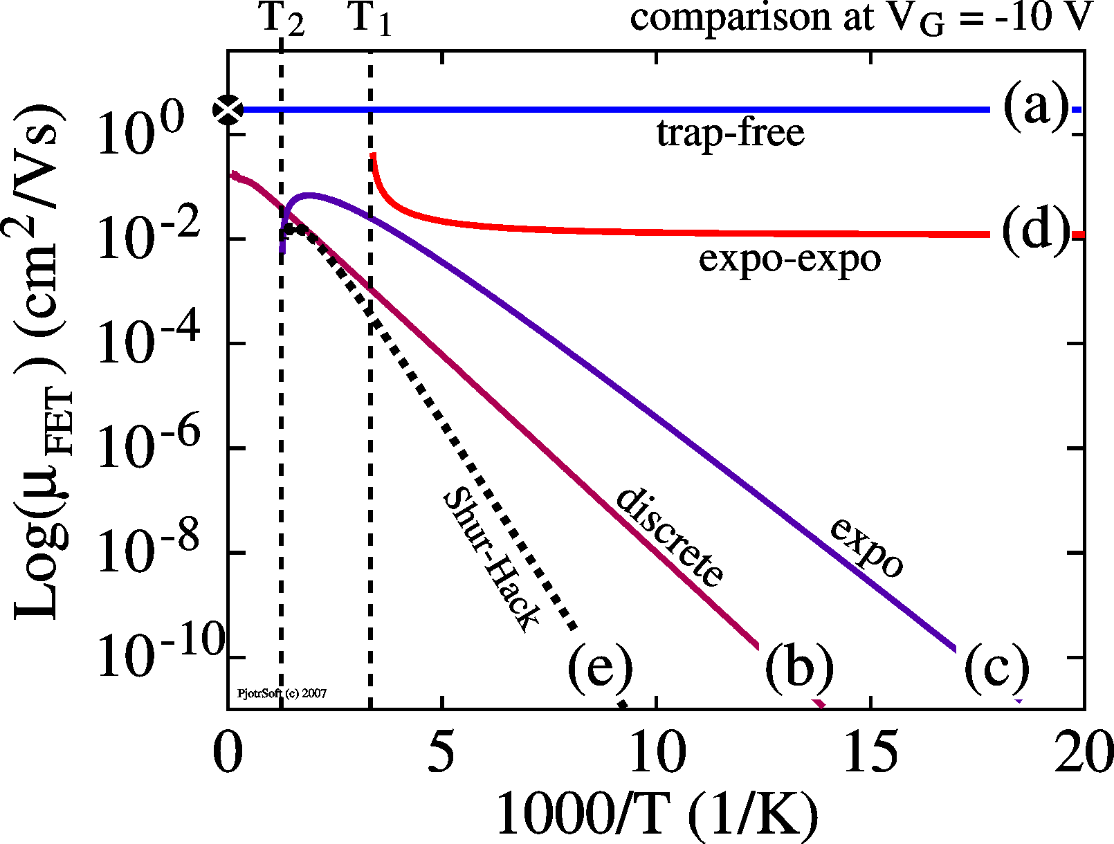
Trap free device. The
(as-measured) mobility is constant - independent of temperature (the Arrhenius plots are horizontal lines; EA = 0) - independent of bias (the activation energies are 0 for all Vg, see inset) The IV and transfer curves are as described above in "the basic model". |
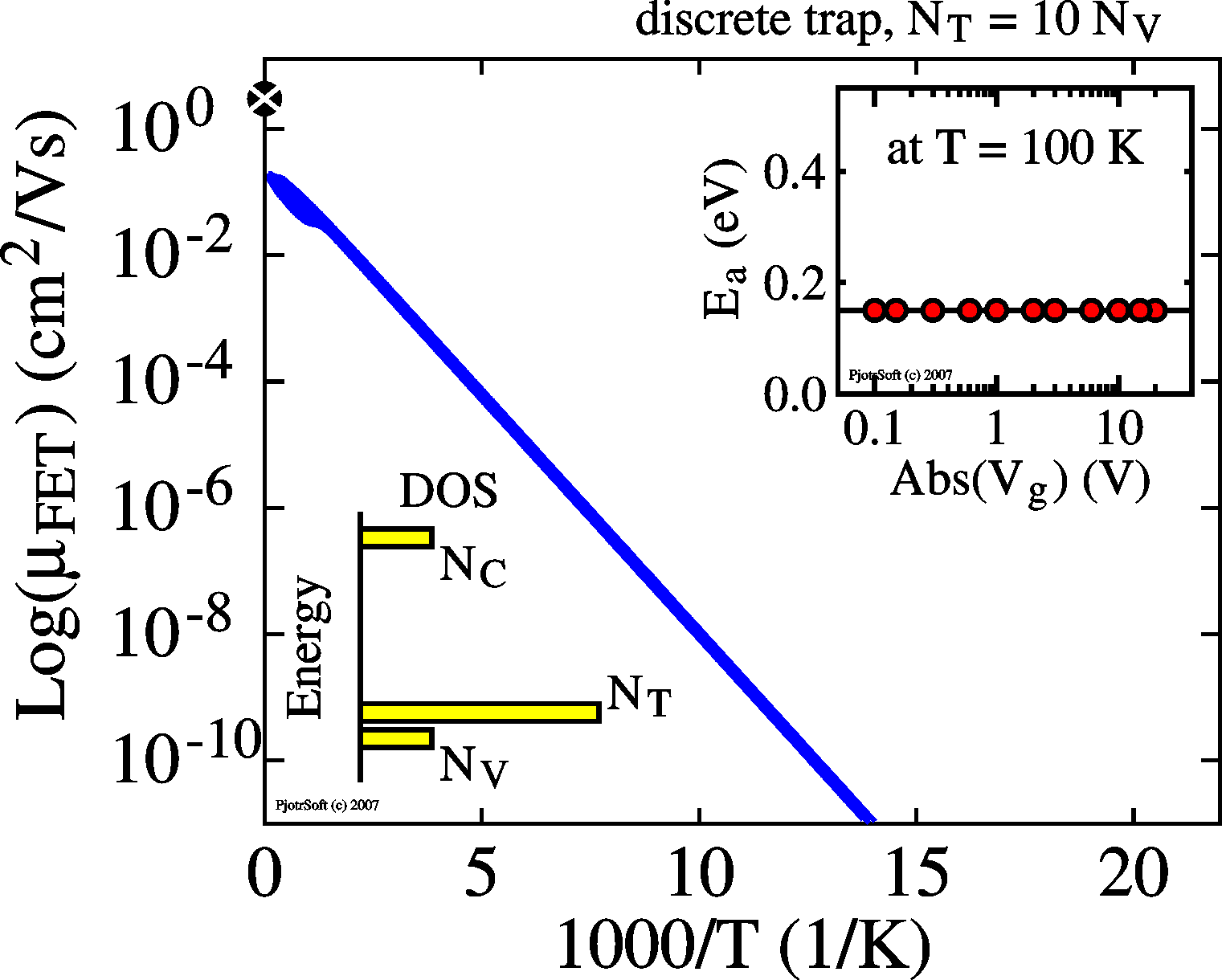 |
With a huge density of discrete
traps, a substantially amount of the charge induced
by the gate bias is on the traps and doesn't contribute to
current. In thermal equilibrium the ratio of free (p) to trapped (pT) charge
follows a Fermi-Dirac distribution. For huge densities of
traps this can be approximated by a Boltzmann distribution.
Thus p/pT
= (NV/NT) *
exp(-ET/2kT)
with NT
the density of trap states and NV the desnity of conductive
states. The total charge induced by the gate is the sum of
trapped and mobile charge (in equilibrium). The current is
proportional to p.
The result is that both the current and the mobility become
temperature dependent with the activation energy found in an
Arrhenius plot equal to half the trap depth ET,
independent of Vg.
However,
|
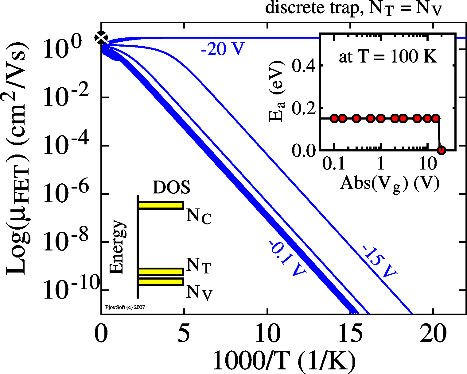 |
When the density of traps is
roughly equal to the density of conductive states (for
instance valence band) the Arrhnius plot resemble
those above, up to a certain gate bias Vg. After
this bias, the trap-free limit Vtfl, the
behavior is as in a trap-free device, with a mobility
independent of temperature and bias.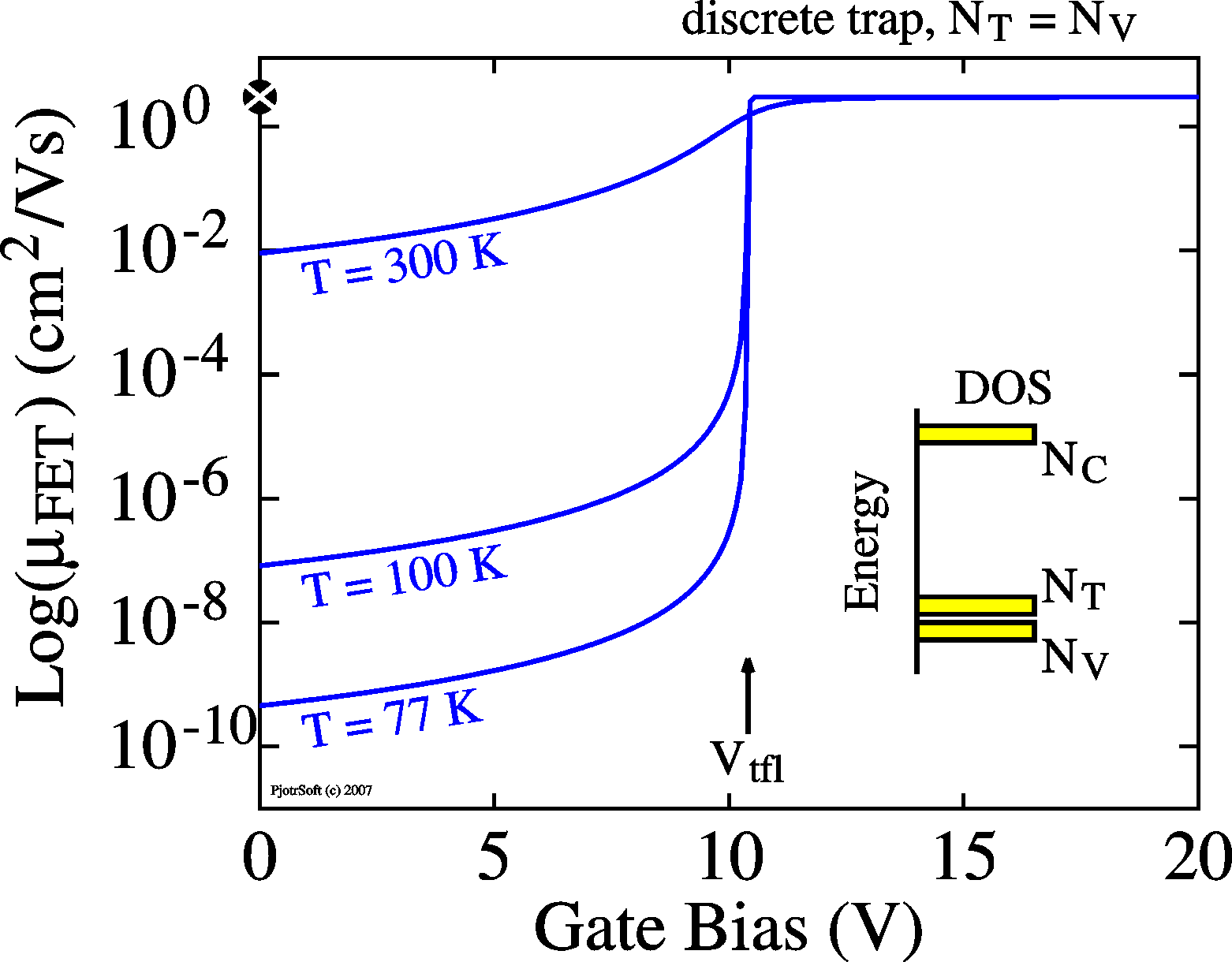 |
 |
For a trap
exponentially distributed in energy (DOS
schematically shown in yellow), the mobility becomes bias
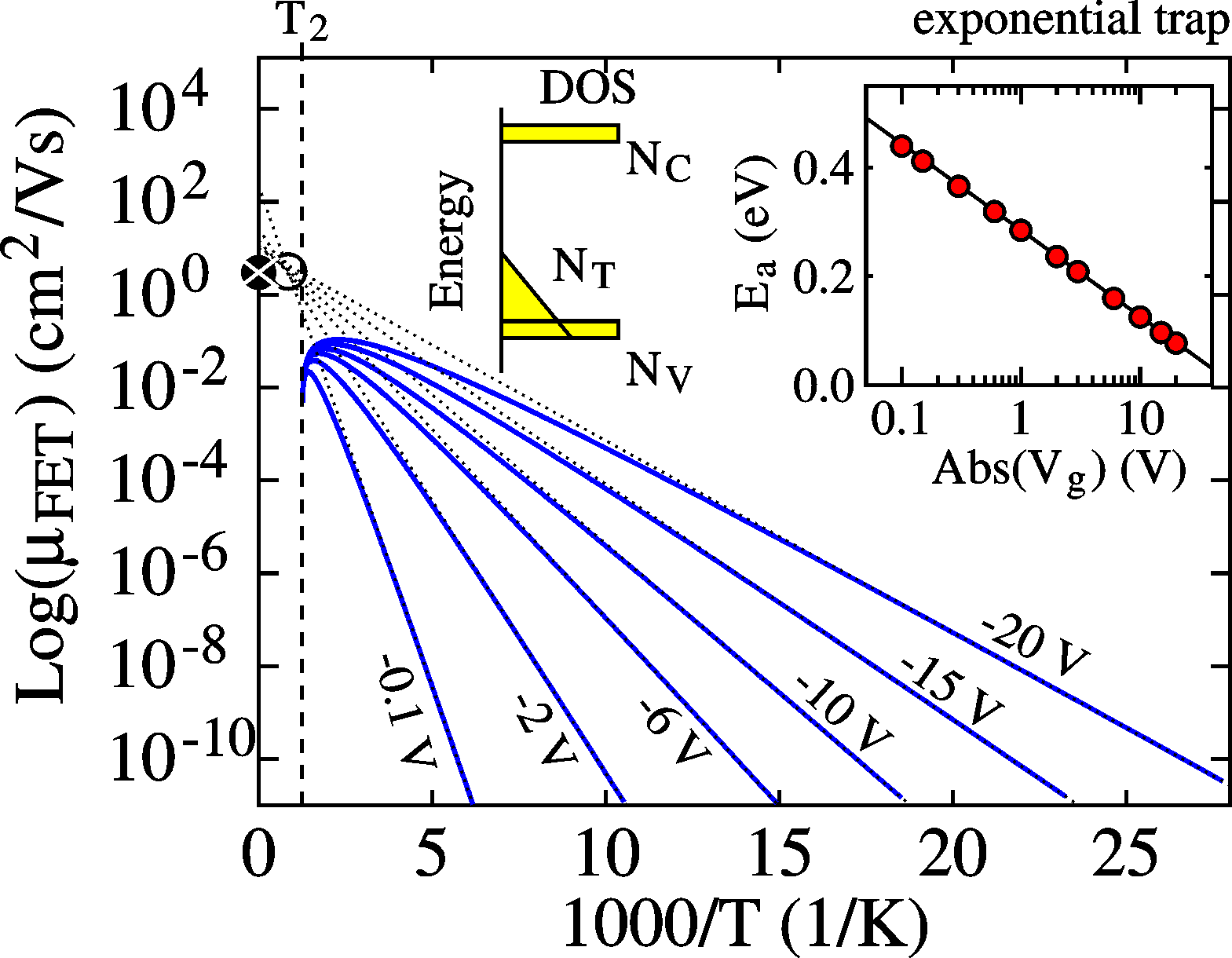
and temperature dependent, resulting in so-called Meyer-Neldel Rule: the
Arrhenius plots all point to a single point, the iso-kinetic
temperature and mobility. |
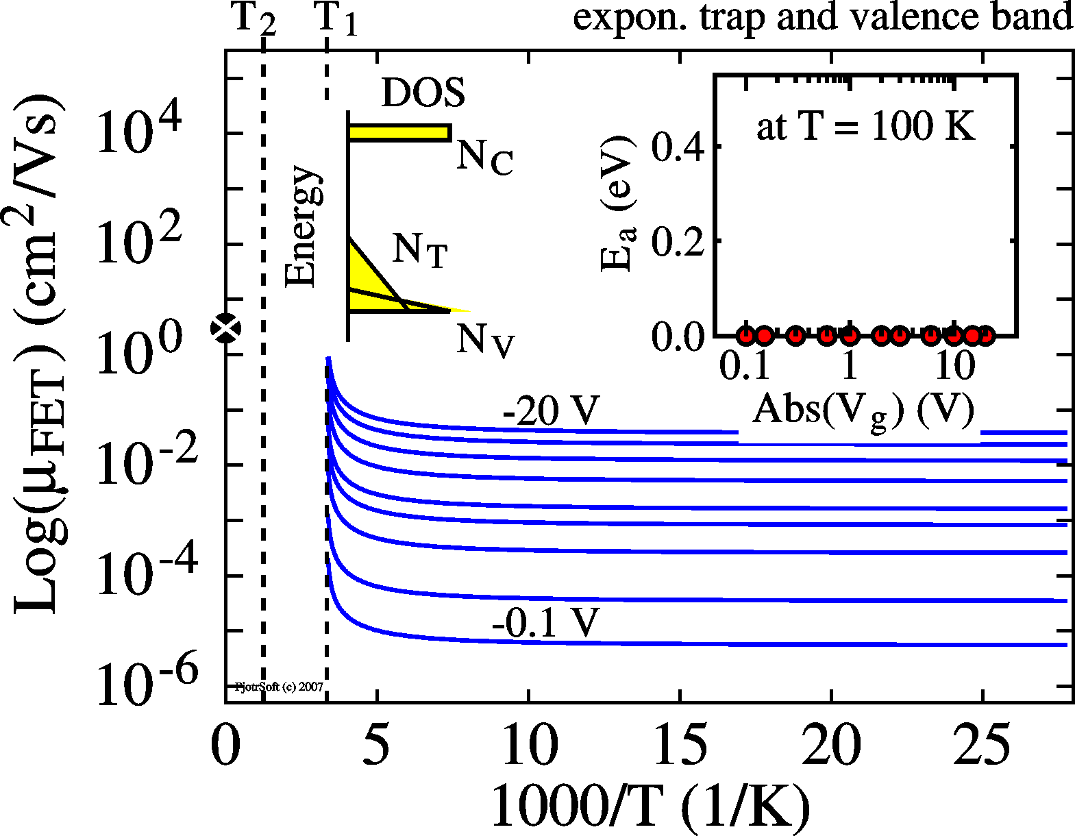 |
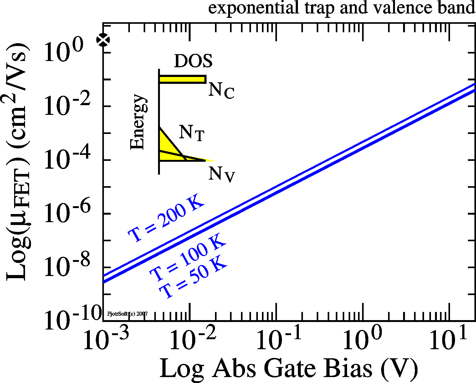 When also the conductive states have an
exponential distribution in energy, the mobility
becomes independent of temperature but remains strongly
dependent on bias. When also the conductive states have an
exponential distribution in energy, the mobility
becomes independent of temperature but remains strongly
dependent on bias.
|
| Simple exponential |
Multi-exponential |
 |
 |
 |
 |
 |
 |