|

Theory of electrical characterization
of (organic) semiconductors
by Peter
Stallinga
Universidade
do Algarve
|
Index:
Preface
The following text is intended to help in understanding the
electrical measurements on semiconductors. In the time that I have
been working here in Faro I have made notes about the measurements
and made them into a file. I thought it would be nice if I share the
accumulated knowledge with others.
With the help of the text, you will be able to understand most of
the electrical measurements of other people. Also, the text can
function as a starting point for new researchers in the area.
The text is not complete. Also, the text is probably full of typos
and mistakes in the equations. If you have any comments please
e-mail me (see e-mail address at end).
These pages need a recent browser. Without it you will not be able
to see the equations correctly. (In older versions there is no
possibility to display Greek symbols or sub- and superscript). The
pages were written with Netscape Communicator 4.76. Some of the
pictures look bad on screen, some bad on the printer. It is not
possible to have high quality images for both output devices at the
same time. Use "view image" to see an enlarged picture when the
screen quality is insufficient in normal viewing mode.
© The copyright of this document belongs to the University of
the Algarve. Please give due credit when using this document. It
helps my career.
P.S., Faro, 2001-2007
Introduction
A good question is: how can a polymer be a metal? Our daily life
experience tells us that polymers ("plastics") are very good
isolators. Indeed, the conductive properties of organic materials
were discovered by accident (see Scientific American of July
1995  );
not many people expected such properties. The obvious answer to the
question is that the conducting polymers have an abundance of free
(or very loosely bound) electrons.
);
not many people expected such properties. The obvious answer to the
question is that the conducting polymers have an abundance of free
(or very loosely bound) electrons.
| Then the next question is: why are some organic materials
(polymers) semiconductors? The answer is well described in
section IVB of Chapter 2 of "Advances in Synthetic Metals,
Twenty years of Progress in Science and Technology"
for the basic conducting polymer poly acetylene. In all
systems of conductive organic materials, the conducting
chain or "backbone" of the molecule consists of unsaturated
carbon atoms (example --CH-CH-CH--; each atom is only
threefold coordinated). Each carbon atom contributes a
single pz-electron to a bond with the neighboring
atoms. This situation is unstable to small
symmetry-breaking distortions (so called Jahn-Teller).
In this case an alternating shortening and lengthening of
the bonds, or alternating double and single bonds. The band
gap that is opened up by this symmetry lowering is in the
order of 2.5 eV and this is still in the range of
semiconductors. The table gives a comparison of the band gap
of various semiconductors. Organic semiconductors mostly
fall in the category "wide-band-gap semiconductors". |
| material |
band gap |
| diamond C |
5.47 eV |
| GaN |
3.36 eV |
| polymer |
2.5 eV |
| GaAs |
1.42 eV |
| Si |
1.12 eV |
| Ge |
0.66 eV |
|
With a bandage of 2.5 eV the polymer would not be conducting at
all. This distance between the valence band and conduction
band is much too large to allow for free carriers to be generated
at room temperature. For that too happen, an electron would
have to acquire huge thermal energy to make the jump to the
conduction band. There are still some ways that we can have free
carriers in the polymer:
- injection of carriers from metallic electrodes or materials
with large amounts of free carriers (for example silicon, or a
conducting polymer)
- optical excitation; creation of electron-hole pairs
- doping. The levels of the dopant can be much closer to either
band and free electrons or free holes are more easily generated
even at low temperatures.
Most organic semiconductors have a sufficient doping level to make
them p-type (abundance of free holes), although for the most pure
ones, the density of free holes is rather small and these can still
be considered isolators.
After having answered the question where the conductance is coming
from the next question is how the conductance looks. There are
models with polarons, bipolarons, etc.
In classic semiconductors, the free electron and hole can bind to
each other (on basis of their electrostatic [Coulomb] attraction)
forming excitons which are hydrogen-like states of the electron
around the hole. Due to the low mass of the hole, the binding energy
of these excitons is very small (meV's). The exciton can also be
bound to a defect and the energy of the system can then be further
reduced. In classic semiconductors these energies are rather small,
but in polymers, these energies can be huge and mid-gap states can
result.
For the theory presented here it doesn't matter what shape the
carriers take. We will assume that all carriers are free
carriers. One important difference between classical
semiconductors and polymers is worth to be pointed out here,
though. In classical materials, the conduction is always
3-dimensional, while polymers are 1-dimensional conductors. Or, at
least there is an anisotropy; the conduction in one dimension is
better than in the other two. Hence, there exist (at least) two
processes for conduction with two activation energies. One for
conduction along the chain and one for "hopping" to near chains.
Device structures
From the semiconductors we can make several types of devices. The
simplest one is a device with only ohmic (non-rectifying)
contacts. This can already give valuable information because
we can measure the conduction model (for instance, number of
conduction processes) or the mobility in Hall
experiments. A little more complicated are Schottky barriers.
They contain a single rectifying contact which can be used to probe
the deep and shallow levels (via IV curves, CV curves, DLTS and TSC,
for example). p-n junctions are very similar to Schottky barriers,
but they can inject with ease electrons into the polymer. Finally we
can make field-effect transistors (FETs) which will yield the
mobility of the carriers.
Ohmic contacts, bulk samples
The simplest device structure is the bar of semiconductor with two
electrodes connected via ohmic (= non-rectifying) contacts. Such a
simple structure already has complicated laws of physics.
The conductivity s of a bar of p-type
material is given by
s = e mp p
with e the elementary charge, mp
the
(hole) mobility and p the hole density. Because both
the free-carrier density mp
and the carrier
mobility p are a function of temperature, the conductivity is
strongly temperature dependent. In fact the hole density (given here
without derivation, see Chapter 1 of Sze ) is equal to
p = 2-1/2 (NANV)1/2
exp(-EA/kT)
~
T3/4 exp(-EA/kT)
Here NA is the acceptor concentration, NV
the density of states at the top of valence band, EA
the activation energy of the acceptor, k the Boltzmann
constant and T the temperature.
The hole mobility depends on the limiting mechanism. We can have the
following models:
| acoustic phonons: |
mp ~ m*-5/2T-3/2 |
| ionized impurities: |
mp ~ m*-1/2T3/2 |
| optical phonons: |
mp ~ m*-3/2T1/2 |
In principle we can determine the activation energy for bulk
conduction through the measurement of the conductivity as a
function of temperature. Normally the resistivity is measured with
a four-point probe. Two points are applying a current and
two other points are measuring the voltage.
The resistivity of the sample in the simple model does not depend
on the voltage. In more sophisticated models it does, but
they will not be described here.
If we know the parameters of the device we can find the mobility
directly from the DC measurements. Otherwise, we have to resort to
FETs, Hall measurements, or Time-of-flight measurements, see the
chapter on measuring mobility.
For insulating materials, the transport can be of yet another
type. In general, it has a stronger field-dependence. Examples:
Fowler-Nordheim tunneling
J = J0 E2 exp(-E0/E)
Poole-Frenkel
J = J0 E exp(sqrt(qE/pe)/kT)
with E the electric field, E = V/d.
In some cases, this is applicable to organic materials in LEDs.
These are normally devoid of free carriers and, especially in view
of the wide bandgap of some of these materials, can be considered
insulators.
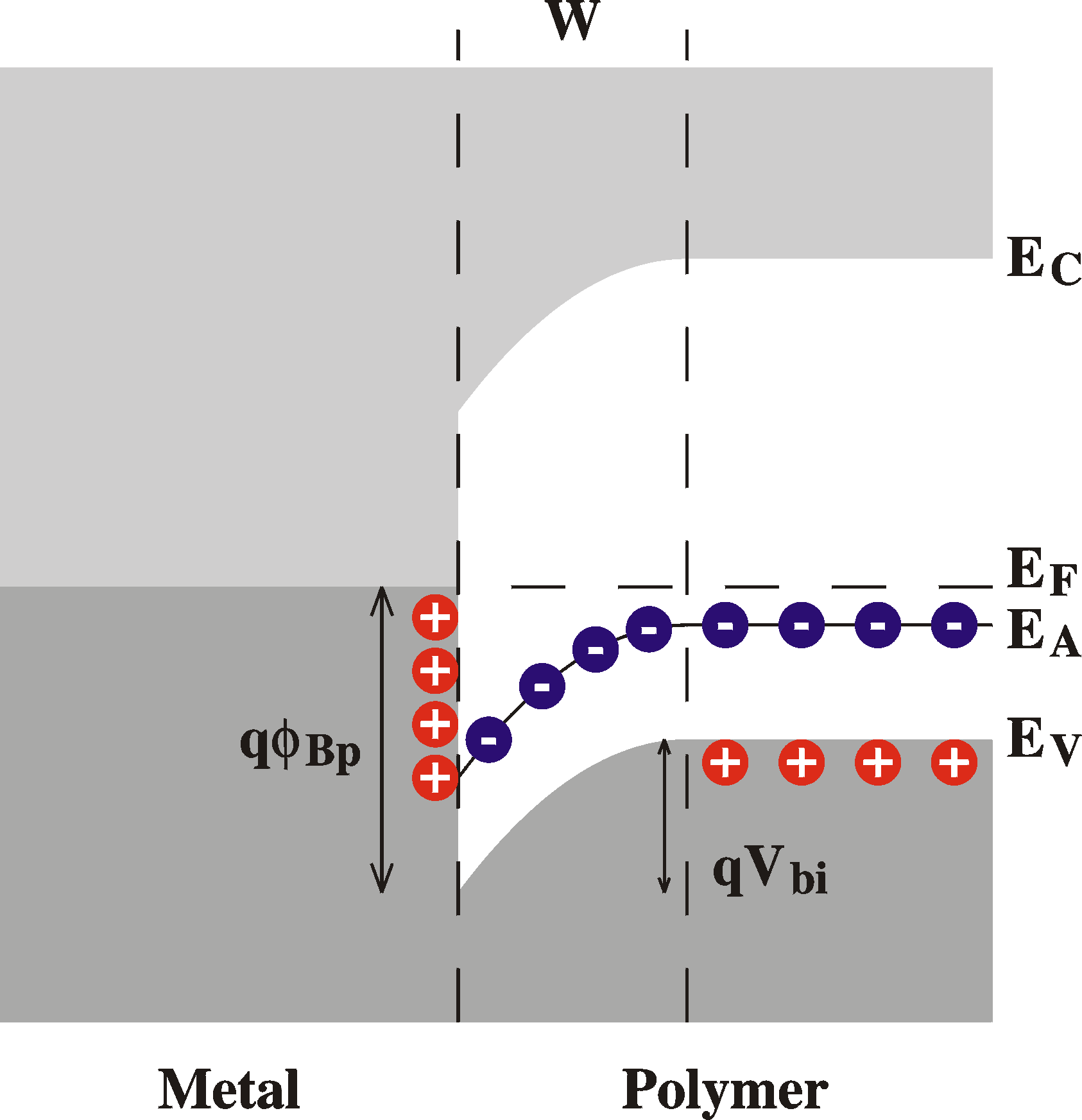
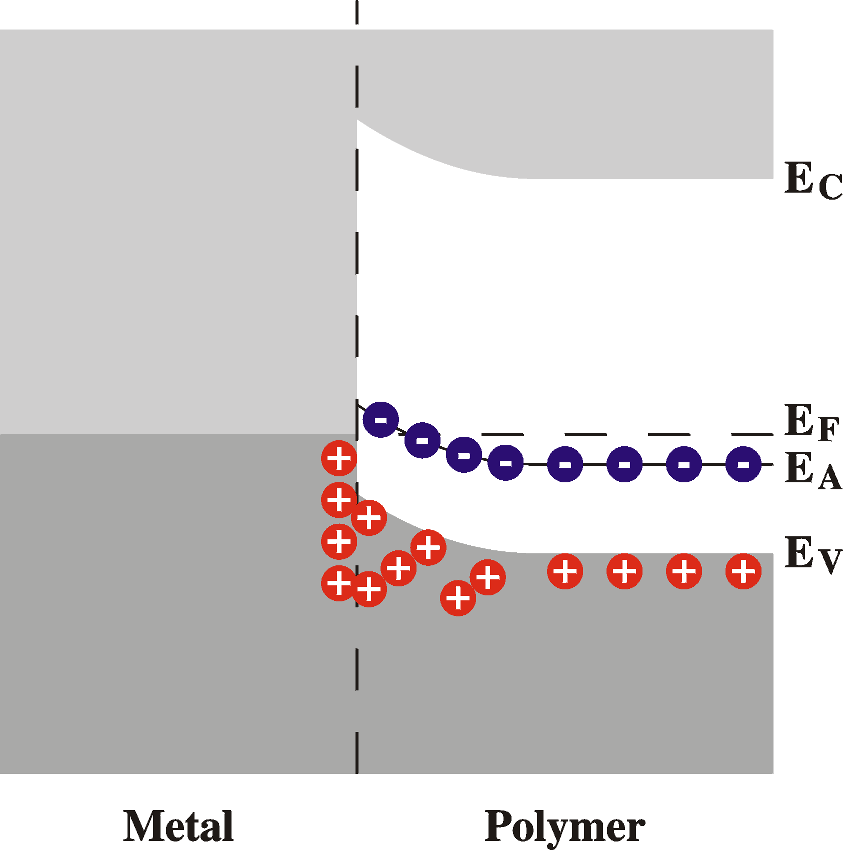
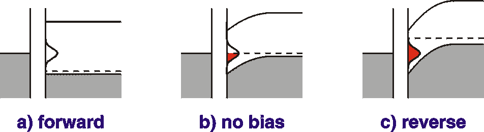
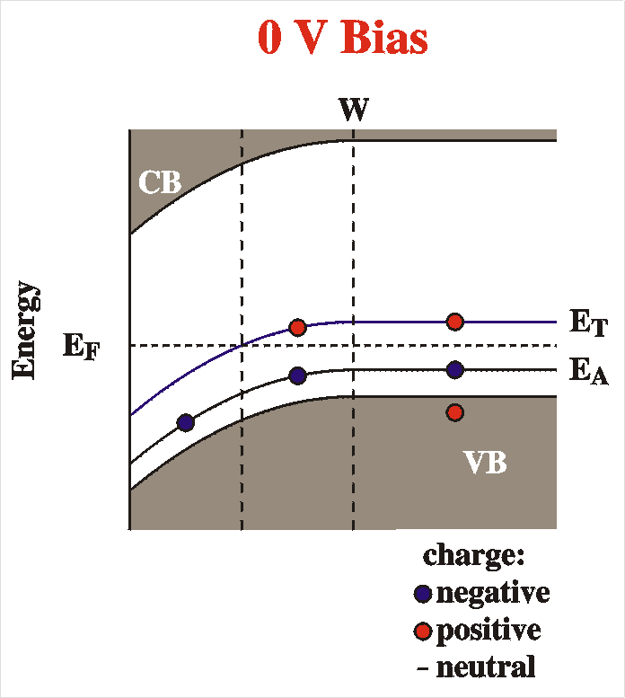
Schottky Barrier
A Schottky barrier is created by the intimate contact of a metal and
a semiconductor surface. The Figure shows the situation of a
Schottky barrier of a metal and a p-type semiconductor, for instance
the polymers P3MeT or MEH-PPV used in our studies. The left drawing
shows the situation before contact and the right drawing the
resulting Schottky barrier after contact.
 |
 |
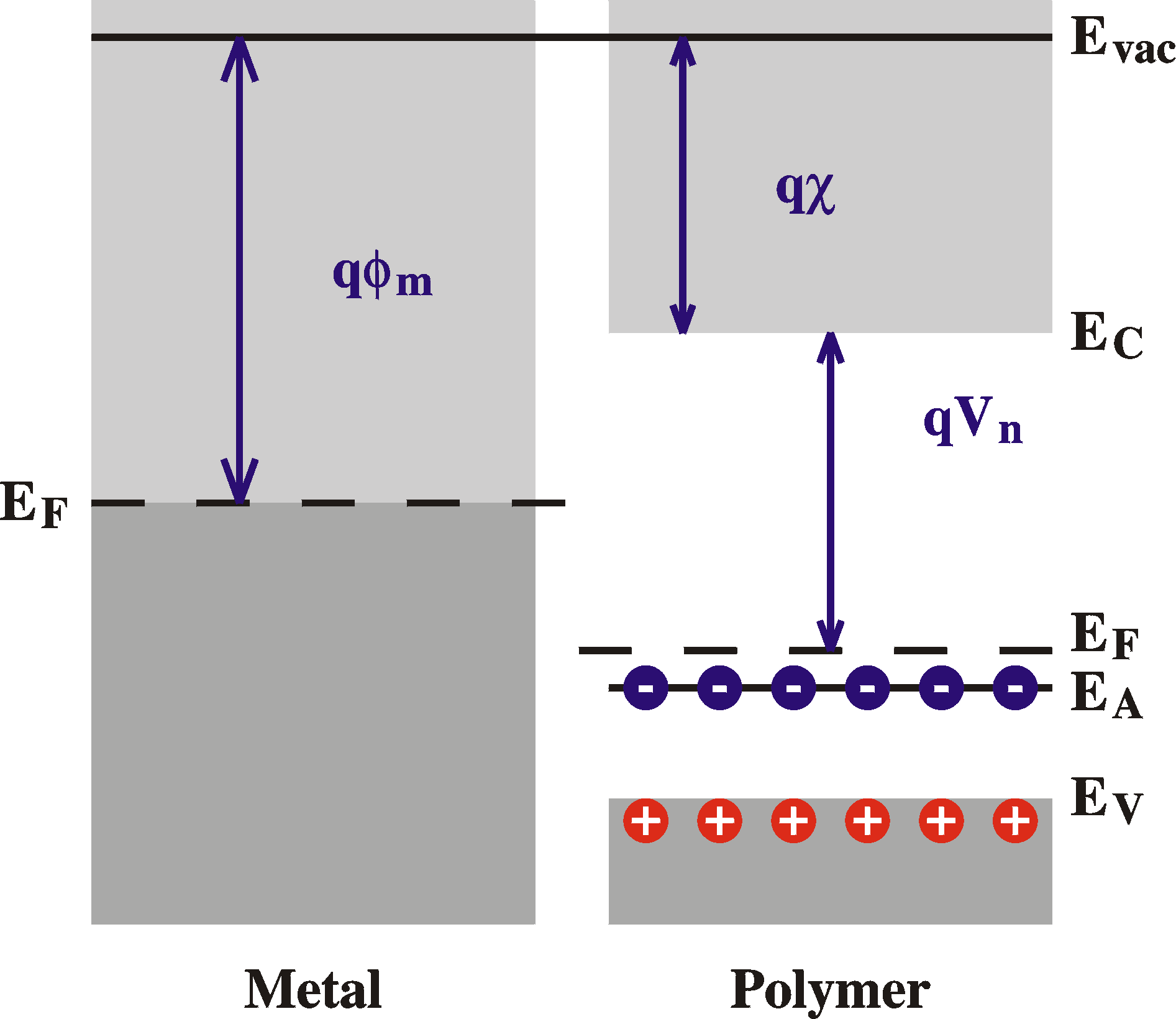
A metal and a semiconductor before contact. Note
the different Fermi levels which will cause electrons
to flow to the semiconductor. |
A Schottky barrier formed after contact of the
metal and the semiconductor. A region of un-
compensated charged acceptors results. This
"space charge" causes a voltage drop at the
interface. |
At equilibrium, in the absence of externally applied voltages,
the Fermi level must be constant throughout the sample, since
otherwise a current would flow. In the metal the Fermi level is
the top of the electron sea, while in the semiconductor, far from
the interface, the Fermi level is determined ("pinned") by the
impurity level. The Fermi level is matched in the following way:
Before equilibrium, the Fermi level is lower in the semiconductor
(when the work function of the polymer, Evac-EF = c + Vn, is larger than
that of the metal, fm),
therefore, electrons will flow from the metal to the polymer. This
causes the build up of charges on both sides of the interface,
resulting in an electric field and therefore a potential gradient
according to Poisson's equation d2V/dx2
= r(x)/e.
This
is the so-called band bending. In this region, the electric field
has caused the holes to move away from the interface; they drift
to the top of the valence band. The result is that in this area --
of width W -- there is a surplus of negative charge
caused by uncompensated charged acceptors, the "space charge
region" or "depletion region", since there is an absence of
majority carriers (holes in p-type semiconductors).
The parameters that describe the Schottky barrier are:
- fBp : barrier
height. The barrier as seen by (majority) carriers coming
from the metal. It depends on the difference in electron
affinity of the metal and the semiconductor and (for p-type
semiconductors) also depends on the energy gap Eg
= EC - EV:
fBp = c + Eg-fm
It is independent of the position of the Fermi level in the
semiconductor and thus on the presence of impurities, etc.
It might be lowered by the so-called image-force-lowering effect
which adds to the energy scheme the potential caused by the
interaction of the charge with its image (virtual) charge on the
metal.
- Vbi : built-in voltage or zero-bias
band bending. The barrier as seen by (majority) carriers going
into the metal. This is determined by the difference in Fermi
level before contact:
Vbi
= (Evac -EF)semicon
- (Evac-EF)metal
=
c + Vn - fm
- W: depletion width. The width of the area devoid
of (majority) carriers. The depletion width can be calculated
when the doping profile is known (as will be shown in the next
section).
For a Schottky barrier the forward bias is when a positive voltage
is applied to the (p-type) semiconductor and a negative voltage to
the metal. This will compensate the band bending and diminish the
barrier.
Similar to the Schottky barrier we have a pn-junction (of two
equal semiconductors with different doping details) or a
hetero-junction (of two different semiconductors). The
theory of these devices is rather similar and will not be
mentioned here further.
Calculation of the depletion width
of a Schottky barrier
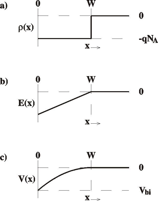 The depletion
width of a Schottky barrier can be calculated from Poisson's
equation
d2V/dx2 = r(x)/e Eq.1
with r(x) the space charge
density at position x. In a first approximation we can
assume a rectangular distribution of the space charge. This is valid
when the acceptors are all ionized and the free charges have moved
out of the interface region leaving behind the now uncompensated
ionized acceptors exactly up to a certain point W, see the
first figure of the section with the Schottky
barrier. In an equation:
r(x) = qNA
for
x <= W
The depletion
width of a Schottky barrier can be calculated from Poisson's
equation
d2V/dx2 = r(x)/e Eq.1
with r(x) the space charge
density at position x. In a first approximation we can
assume a rectangular distribution of the space charge. This is valid
when the acceptors are all ionized and the free charges have moved
out of the interface region leaving behind the now uncompensated
ionized acceptors exactly up to a certain point W, see the
first figure of the section with the Schottky
barrier. In an equation:
r(x) = qNA
for
x <= W
r(x) =
0
for x > W
(see the Figure). In that case the electric field can be
calculated by integrating Eq. 1:
E(x) = dV/dx = (qNA/e) (x-W)
where the boundary condition E(W) = 0 was used. The voltage can then
be found by integrating this equation to give:
V(x) = (qNA/2e) (x-W)2
(boundary condition V(W) = 0). At x=0 the
voltage must be equal to the built-in voltage, Vbi,
therefore:
Vbi = qNAW2
/ 2e and Eq.2
W = (2eVbi /
qNA)1/2
When bias is applied to the device the voltage at x=0 should be
equal to Vbi-V,
therefore:
W = [2e(Vbi-V)/ qNA]1/2 Eq.3
Capacitance of a Schottky barrier
When the bias voltage on the device is changed, a new equilibrium
state will be reached with a new amount of space charge as described
above. The AC capacitance of a Schottky barrier can be defined
as the incremental change of space charge Q in the depletion
range upon an incremental change of voltage, C = dQ/dV.
Note that this capacitance can depend on the applied voltage, in
contrast to normal capacitors which have a constant C = Q/V.
For the rectangular distribution described above, Q equals qNAWA,
with A the active area of the device, and the potential was
given by Equation 2, therefore
C = dQ/dV = d(qNAWA)
/ d(W 2qNA/2e) = eA/W
This relation is in fact a very important one. The capacitance
is determined completely by the width of the depletion region:
C = Ae/W
This shows that a Schottky barrier behaves like a capacitor made of
parallel plates with area A, spaced W and filled
with a dielectric medium e. Substituting
the calculated depletion width from Equation 3 also gives
C = A [qeNA / 2(Vbi-V)]1/2
 This shows that a
Mott-Schottky plot (C -2
vs. V) is a straight line and the slope reveals the acceptor
concentration.
C -2 = 2(Vbi-V)
/ A2qeNA
In the same plot, extrapolating to C -2=0 reveals the built-in voltage and
hence the barrier height (if the shallow level depth is known). It
is important to note that NA stands for the
density of ionized acceptors (and impurities). For normal
shallow acceptor levels this is equal to the acceptor density, but
for deeper levels it can be the case that they are only partially
ionized. The capacitance (and depletion width) sees only the ionized
defects. A capacitance transient for instance, monitors the change
in density of these ionized defects.
This shows that a
Mott-Schottky plot (C -2
vs. V) is a straight line and the slope reveals the acceptor
concentration.
C -2 = 2(Vbi-V)
/ A2qeNA
In the same plot, extrapolating to C -2=0 reveals the built-in voltage and
hence the barrier height (if the shallow level depth is known). It
is important to note that NA stands for the
density of ionized acceptors (and impurities). For normal
shallow acceptor levels this is equal to the acceptor density, but
for deeper levels it can be the case that they are only partially
ionized. The capacitance (and depletion width) sees only the ionized
defects. A capacitance transient for instance, monitors the change
in density of these ionized defects.
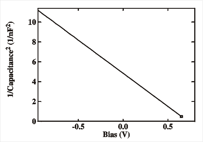
The Figure shows an example of a system with an acceptor
concentration of 4.28 1015 cm-3
and a built-in voltage of 0.75 V.
Capacitance in the case of non uniform
doping
In case of a nonuniform doping profile, the relation Q = qNAWA
no longer holds. Instead we have to use Q =  qNA(x)Adx.
The calculation of the depletion width is also different, but the
relation C = eA/W is
still valid. The end result is that the slope in a Mott-Schottky
plot still reveals the acceptor concentration but locally at the end
of the depletion width and the slope can therefore change with
voltage:
dC -2 /dV
= -2V / A2qeNA (x
= W = eA/C)
This enables the determination of the doping profile NA(x)
through the CV measurement. The depth x is determined by the
measured capacitance and the dopant density at that place is
determined by the measured derivative.
qNA(x)Adx.
The calculation of the depletion width is also different, but the
relation C = eA/W is
still valid. The end result is that the slope in a Mott-Schottky
plot still reveals the acceptor concentration but locally at the end
of the depletion width and the slope can therefore change with
voltage:
dC -2 /dV
= -2V / A2qeNA (x
= W = eA/C)
This enables the determination of the doping profile NA(x)
through the CV measurement. The depth x is determined by the
measured capacitance and the dopant density at that place is
determined by the measured derivative.
Numerical calculation of the depletion layer
Alternatively we can describe the depletion layer in the following
way. Instead of defining the origin x=0 at the interface, as
described above, it can also be defined as the start of the
depletion layer. In that case,
E(x) = dV/dx = (qNA/e)x
V(x) = (qNA/2e)x2
At the interface (x=W), the potential should be equal
to the band bending (VS = Vbi-V):
V(W) = (qNA/2e)W
2 = VS
W = (2eVS / qNA)1/2
If V is increased with an amount DV,
charge will flow into the interface and the depletion width will
shrink. This happens at x=W (in this equation):
C = dQ/dV|x=W
=
(dQ/dx)(dx/dV)|x=W
which should be evaluated at x=W. Note that dQ/dx
equals Ar and dV/dx
equals E(x), therefore
C = Ar/E(W)
= A qNA / (qNA/2eVS)1/2
= A [qeNA /
2(Vbi-V)]1/2 Eq.4
as found before. This method only works for homogeneous
distributions in space, when it is unimportant from which side you
start your calculation. This is especially useful when you do
numerical integration, since the values (V, E) at the
starting point (x=0) do not depend on the end of the
depletion width (x=W). It is still very easy to
calculate the capacitance, even when there is a complicated
distribution of levels in energy. The computer can integrate until
the cumulative band bending reaches the input parameter VS.
At that point the electric field E and charge density r can be evaluated and the capacitance
calculated
according to Equation 4.
The Figure above shows an algorithm used for calculating
depletion widths and capacitances for Schottky barriers ("view
image" to see it in more detail). As an example, consider
the situation of a system with two homogeneously distributed
acceptor
levels, one 0.1 eV and the other 1.0 eV above the valence band
with the Fermi level at EVB + 0.6 eV. Both have
a concentration of 1016 cm-3.
For e=5, a dot diameter of 2 mm, and a
built-in voltage of 0.8 V, the Mott-Schottky plot is given in the
Figure.
 The
Figure shows a simulation of a C-2V
plot of a two-level system as described in the text. For voltages
higher than 0.4 V (built-in voltage - ET1-EF
the band bending is not large enough to put the deepest level
below the Fermi level anywhere. Hence the space charge is only a
result of the shallow level and we see a large slope (small
concentration). For lower voltages, or reverse voltages, both
levels contribute to the space charge and both are visible in the
slope which is now much smaller. Note that the sharpness of the
transition is due to the assumption that around the Fermi level
the levels are either completely full or completely empty
(emulating 0 K). The situation for T=300 K is shown with a
dashed line. Note also that the two slopes do not point to the
same built-in voltage Vbi. The slopes will
still yield the correct acceptor concentrations, though.
The
Figure shows a simulation of a C-2V
plot of a two-level system as described in the text. For voltages
higher than 0.4 V (built-in voltage - ET1-EF
the band bending is not large enough to put the deepest level
below the Fermi level anywhere. Hence the space charge is only a
result of the shallow level and we see a large slope (small
concentration). For lower voltages, or reverse voltages, both
levels contribute to the space charge and both are visible in the
slope which is now much smaller. Note that the sharpness of the
transition is due to the assumption that around the Fermi level
the levels are either completely full or completely empty
(emulating 0 K). The situation for T=300 K is shown with a
dashed line. Note also that the two slopes do not point to the
same built-in voltage Vbi. The slopes will
still yield the correct acceptor concentrations, though.
DC: Current through a Schottky barrier
According to thermionic emission theory
J = A*T 2exp(-qfBp/kT
) [exp(qV/kT) - 1],
with A* the Richardson constant,
A* = 4pqm*k2/
h3
(q is the elementary charge = 1.60217733 10-19 C, k is the Boltzmann
constant = 1.380658 10-23 J/T,
T is the absolute temperature in Kelvin, V the bias
voltage in volt, fBp is the
barrier height in volt, and h is Planck's constant =
6.6260755 10-34 Js).
Alternatively, the current can be following the diffusion
theory:
J = { (q2DnNC
/ kT) [(2qND/e)(Vbi-V)]1/2 exp ( -qfBp/kT)}[exp(qV/kT) -
1],
Finally, a combination of the two theories, the thermionic
emission-diffusion theory predicts a current following the
equation
J = A**T 2exp(-qfBp/kT
) [exp(qV/kT) - 1],
with A** the effective Richardson constant.
The currents are all of the form
J = J0 [exp(qV/nkT)
- 1]
In this n is the ideality factor (>1), parametrizing the
deviation from theory. For classic semiconductors such as Si, Ge or
GaAs the value of n is close to 1, while for polymers it is
often in the order of 2.
|
thermionic-emission theory
|
diffusion theory
|
 |
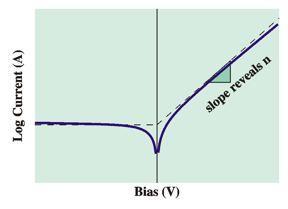 |
From a DC current-voltage plot ("IV plot") we can determine
- the ideality factor n from the slope in forward-bias
- the correct model for conduction
- in thermionic-emission theory the reverse current saturates
(levels off)
- in diffusion theory the reverse current depends on the bias
- the saturation current J0 from the
reverse-bias saturation current or the extrapolated-to-zero-volt
forward-bias current.
- the barrier height (fBp)
when the temperature is varied: A plot of ln( J/T
2 ) (or ln (JT) for diffusion theory)
versus 1/T in strong forward bias (so that "-1" can be
neglected) results in a straight line with slope q(V-fBp)/k from which the
barrier height fBp can be
derived. Alternatively it can be done in strong reverse bias, so
that the exponent can be neglected and the slope will be -qfBp/k
J0 ~ T 2exp(-qfBp/kT
)
- The rectification ratio of a device. This depends (for a fixed
voltage, say 1 V) on the J0, also known as
"leakage current".
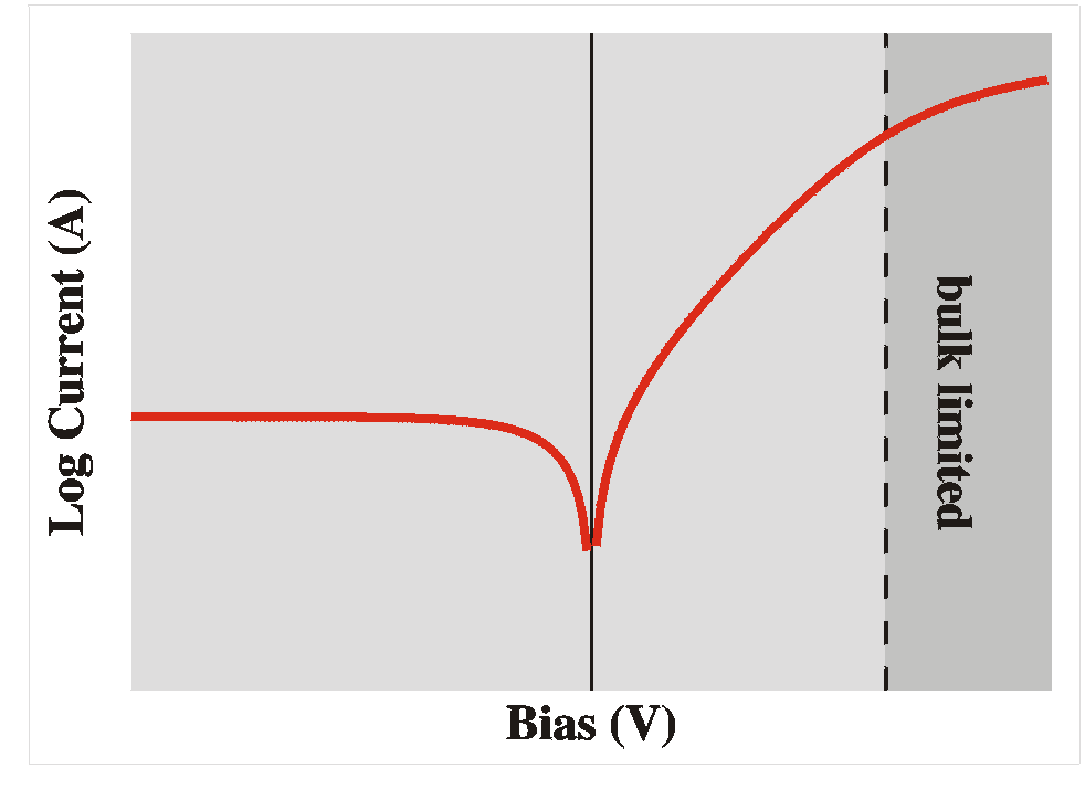 |
A final note: For high forward voltages, the current may
be limited by the resistivity of the bulk. In that case, the
current doesn't continue to rise exponentially with the
bias, but only grows linearly. In the semi-log IV curves
this is visible as a bending of the curve at strong forward
bias.
Since the current is limited by the bulk conductivity we can
again apply the theory for bulk samples. |
Space-charge-limited current (SCLC)
 A special case is when the
currents are limited by the space charge. This means that
the density of free carriers injected into the active region
is larger than the number of acceptor levels. It is easy to
see that we then go from situation of band bending caused by
uncompensated ionized acceptor levels to the case of band
bending caused by over-compensated acceptor levels.
The band bending is then in the other direction (!). The
local field the carriers feel when injected into the active
region is then driving them out of there and back into the
contact electrode. The entire current must come from the
diffusion of carriers. In other words, the current is caused
by the large gradient of density of free carriers. A special case is when the
currents are limited by the space charge. This means that
the density of free carriers injected into the active region
is larger than the number of acceptor levels. It is easy to
see that we then go from situation of band bending caused by
uncompensated ionized acceptor levels to the case of band
bending caused by over-compensated acceptor levels.
The band bending is then in the other direction (!). The
local field the carriers feel when injected into the active
region is then driving them out of there and back into the
contact electrode. The entire current must come from the
diffusion of carriers. In other words, the current is caused
by the large gradient of density of free carriers.
Instead of the simple approximation with only the drift
current
I = qmenE
we have the more complex form including both the drift
current and the diffusion current:
I = qmenE
+
qDn dn/dx
In fact, the drift current is opposing the diffusion current
as can be seen in the figure; the electric field will drive
the holes back to the metal.
In general, we can expect space charge limited currents
(SCLC) when the acceptor density is small (and the
band-bending and E becomes negative for large
amounts of injected carriers) or when the mobility of the
carriers is small (so that the first term in the equation
above becomes negligible compared to the second term),
especially when and where the charge-density gradient dn/dx
is large.
|
The Bell Labs group of Schön and Batlogg gives a nice
summary of these measurements (PRB
58), which, in turn, is based on chapter 7.3.4. of
Sze .
The DC current of a device can be divided into the following
types:
In the Ohmic regime, the current is proportional to the
electric field. This is equal to a simple resistance.
The space-charge-limited-current regime (SCLC) occurs when
the equilibrium charge concentration (before charge injection) is
negligible compared to the injected charge concentration. This
will form a space charge cloud near the injecting electrode; the
concentration of the space charge rapidly dies out away from the
electrode. In this regime, the current is proportional to the
square of the electric field.
With the bias, the trap levels are filled. Above the trap-free
voltage limit, the traps are filled and the device enters
the trap-free SCLC.
The figure below summarizes this.
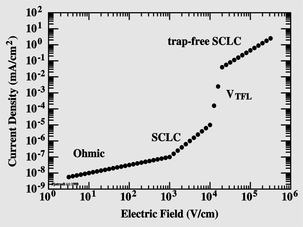 |
Ohmic:
J ~ mV
Space-Charge Limited Current (SCLC):
J ~ mV 2
Trap-Free Voltage Limit (VTFL):
VTFL
~ d2Nt
Trap-Free SCLC:
J ~ mV 2
|
Note that this is the current through a Schottky barrier. That is,
we assume an ohmic contact on one side and a Schottky barrier
metal-semiconductor contact on the other side of the
semiconductor. If we have two Schottky barriers (for instance
because we use the same metal for both electrodes), we get
so-called MSM (metal-semiconductor-metal) devices, which have
different behavior (notably: the current is proportional to V
instead of V 2 according to p. 616 of Sze. Not
true, see p. 478).
Displacement current
As we have seen, the device can have a rather large
capacitance. This capacitance can give valuable information
about the material. In some cases the capacitance of the
interface is obstructing the measurement, though. Imagine measuring
the DC conductance of a capacitor (theoretically zero). Every time
the bias is changed the capacitor has to reach the new equilibrium
amount of charge stored. In other words, charge will flow in to (or
out of) the device and this is the so-called displacement current.
When the scanning speed is large (or the capacitance is large) this
current can be substantial, even overshadowing the DC conductance of
a device.
When the device has a capacitance C and we are scanning with
a speed l = dV/dt, then
the displacement current is equal to
| Idisp |
= |
dQ
|
= |
d(CV)
|
= C |
dV
|
+ V |
dC |
= C |
dV |
+ |
V |
dC |
dV |

|
|
|
|
|
|
|
|
dt
|
dt
|
dt
|
dt
|
dt
|
dV
|
dt
|
| Note that the capacitance of the device also depends on
the voltage (see the section on capacitance)
and this also contributes to the displacement current.
The figure shows an example of a large displacement
current compared to the DC conductance. (Sample:
PMeT/Al, 2mm electrode diameter, dV=10mV, dt=100ms,
T=300K). The points where the current is zero have
moved away from 0 V. For upward scanning, the
displacement current is positive and the situation of
zero current is reached earlier, hence the crossing
point is at negative voltage. For the same reason,
the zero-crossing point for downward scanning moves to
the right.
The obvious remedy is lowering the scanning speed.
|
 |
AC: Conductance of a Schottky
barrier.
Spectra, Loss and Loss-tangent.
The currents in the previous section were static DC currents. For
such currents, the resistance is defined as R = V/J
and the conductance G = 1/R = J/V.
In AC measurements we apply a voltage that is a superposition of a
DC voltage and an AC component v.
V = VDC + v sin(wt)
The resulting current can also be decomposed in a DC and an AC part:
J = JDC + j sin(wt)
JDC is the current of the previous section. The AC
current, j, can easily be calculated if we assume that the
AC voltage v is small. In that case, the current is
proportional to the derivative of the DC current J(V)
times the AC voltage. The conductance is then defined as the ratio
of AC current and AC voltage
G = j/v = dJ/dV
In general G depends on the applied bias (VDC)
as well as the frequency (w). Later, in
the section on admittance spectroscopy we
will see why it depends on the frequency. On the other hand, it is
easy to show why G depends on the voltage. From the
previous section we have
J = J0 [exp(qV/nkT)
- 1]
and therefore the conductance is equal to
G = G0 exp(qV/nkT)
The unit of G is the reciprocal ohm (mho, 1/W)
or siemens (S). In some cases the conductance is expressed in
terms of loss L:
L = G/w = L0
exp(qV/nkT)
whose units are farad (F). In either case, according to
thermionic-emission theory a plot of the logarithm of conductance
(or loss) vs. voltage is a straight line intersecting the vertical
axis at G0 (or L0).
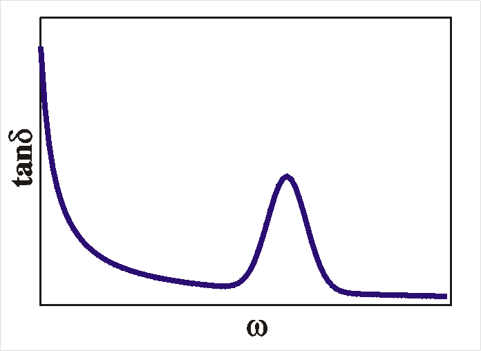
 Finally, we can also define the loss-tangent, tand,
as G/wC. The name
loss-tangent stems from the fact that in a phase plot, the lossy
current, comprised of wC and G,
makes an angle d = tan-1 (G/wC)
with the capacitance axis. For the simple model, the loss tangent
shows no features in the spectra (tand
vs. frequency) and is "flat" (~1/w). We
will now show how deep states can produce peaks in the spectra.
Finally, we can also define the loss-tangent, tand,
as G/wC. The name
loss-tangent stems from the fact that in a phase plot, the lossy
current, comprised of wC and G,
makes an angle d = tan-1 (G/wC)
with the capacitance axis. For the simple model, the loss tangent
shows no features in the spectra (tand
vs. frequency) and is "flat" (~1/w). We
will now show how deep states can produce peaks in the spectra.
Capacitance in the presence of a second
(deep) level
When there are more levels in the forbidden gap the situation
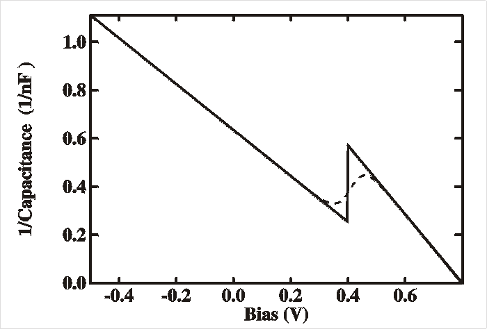
becomes more complex. Consider first the situation of two acceptor
levels, one shallow and one deep. In fact so deep that in the
absence of bias it nowhere drops below the Fermi level. This
implies that all of the deep acceptor levels are filled (with holes)
and are therefore neutral and do no contribute to the space charge
and capacity; the slope in the Mott-Schottky plot represents then
only the shallow acceptor concentration. For strong reverse biases
the increased band bending can force the deep acceptor below the
Fermi level at a region close to
the interface. Now if the level is shallow enough so that it can
respond to the AC probing signal (of the order of 1 kHz) it will
start contributing to the capacitance. The apparent
concentration is then the sum of the two concentrations of the
acceptors.  This
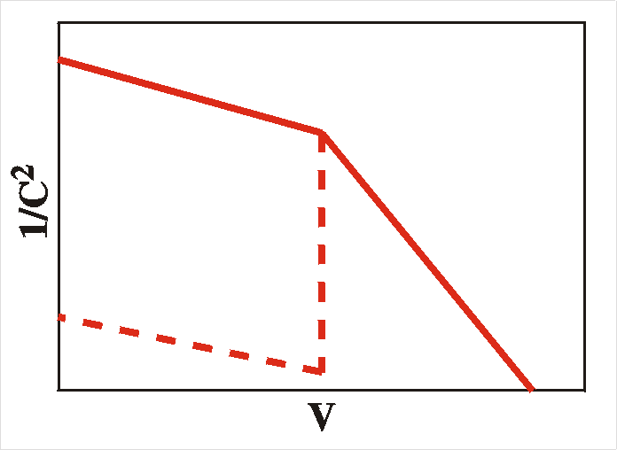
is visible in a sudden drop and a reduction of the slope to 1/(NA1
+ NA2) for biases smaller (more reverse) than Vbi- (EF -EA2)/q,
as is easily seen in the Figure. Also, note that the apparent
built-in voltage seems to decrease; the intersect of the slope with
the voltage axis is lowered to Vbi- NA2(EF-EA2)/q(NA1+NA2).
This
is visible in a sudden drop and a reduction of the slope to 1/(NA1
+ NA2) for biases smaller (more reverse) than Vbi- (EF -EA2)/q,
as is easily seen in the Figure. Also, note that the apparent
built-in voltage seems to decrease; the intersect of the slope with
the voltage axis is lowered to Vbi- NA2(EF-EA2)/q(NA1+NA2).
If the level is too deep and the probing frequency is too high
compared to the characteristic level filling and emptying times
t, it does not respond anymore.
It is still visible in a certain reduction in the slope in the
Mott-Schottky plot, but now without the sudden drop.
Important to note is that the slope is no longer linear and a
straight-line fitting does not reveal the true acceptor
concentration anymore; the Equation found for the derivative found
before is no longer valid. Also, any extrapolation of the
local slope to 1/C2=0 increases to beyond Vbi.
In the presence of a donor level the situation is more complex,
since the position of the electron (quasi) Fermi level is not so
well known. Its position is determined by the number of free
electrons in the conduction band and this depends on many factors
such as the mobility, concentration and life time of these
minority carriers. What we can say is that the Fermi level moves
in the opposite direction compared to the hole (quasi) Fermi
level. When the Fermi level doesn't cross the donor level anywhere
(this is most often the case, especially for shallow donor
levels), the donors just act as compensation for the acceptors and
a reduced acceptor concentration is found in the plots, NA
-ND.
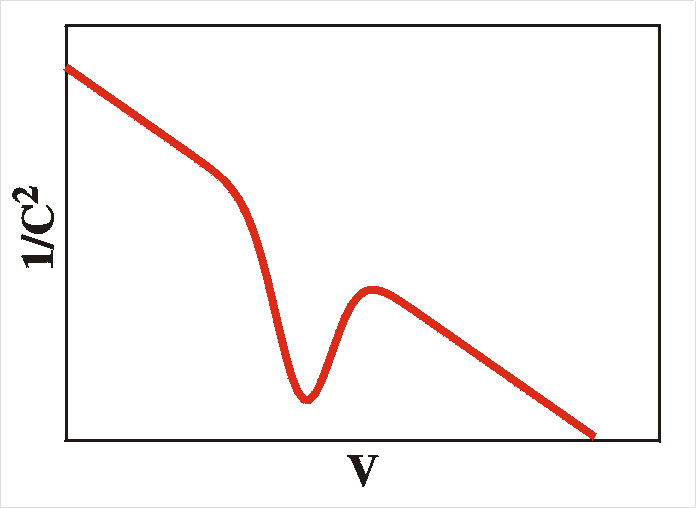
The Figure shows two simulations. In both simulations there are
two levels (one shallow and one deep). In the first simulation the
deep level is responding (dotted line), while in the second it is
non-responding (solid line). The parameters for the simulations
are given in the Table.
| parameter |
value |
| EF |
0.6 eV |
| Vbi |
0.75 V |
| EA1 |
0.12 eV |
| NA1 |
4.28 1015 cm-3 |
| EA2 |
1.35 eV |
| NA2 |
6.272 1016 cm-3 |
| EVB |
0 eV (defined) |
As for the frequency response, we can say the following:
For very low frequencies the deep states have adequate time
to reach thermal equilibrium at all moments and the amount
of charge transferred is proportional to the number of deep
levels and is independent of the frequency. When the
frequency is increased beyond the relaxation time of the
levels (see section on emission and capture
of carriers) the amount of charge transferred is
diminished, simply because the levels have no time to reach
thermal equilibrium. We will measure a much reduced
capacitance and conductance.
To summarize: for deep levels we expect a bend or a drop in
the CV plots and a peak in the loss-tangent (tand = G/wC)
occurs when the radial frequency w
is equal to the reciprocal relaxation time 1/t. |
 |
Interface states
In the above discussion the shallow and deep states were considered
homogeneously distributed in space. As a short excursion,
non-homogeneously distributed shallow levels were described in the
section on non-uniform doping. In the current
section the other extreme will be described, namely levels that have
a delta-function-distribution in space. The levels are only present
at the interface. At first sight, nothing changes in the theory, but
the effects are pronounced in the plots.
At forward bias, the Fermi level is under the interface states
and they are therefore empty (contain no electrons). When the bias
is lowered, there comes a moment where the Fermi level is resonant
with the interface states and they are partly filled. In that
case, when the Fermi level is modulated (by the external bias)
charge will flow into and out of the interface (states). This is
equivalent to a capacitance. Because energy is lost in the
process of moving the charges, part of the current is in-phase
with the external voltage and is therefore observed as
conductance. When the bias is further reduced, the Fermi level is
completely above the interface states and modulating it will have
no effect on the amount of charge present there; no current will
exist that is associated with the movement of charge. We can
therefore expect a peak in the capacitance-voltage (CV) as
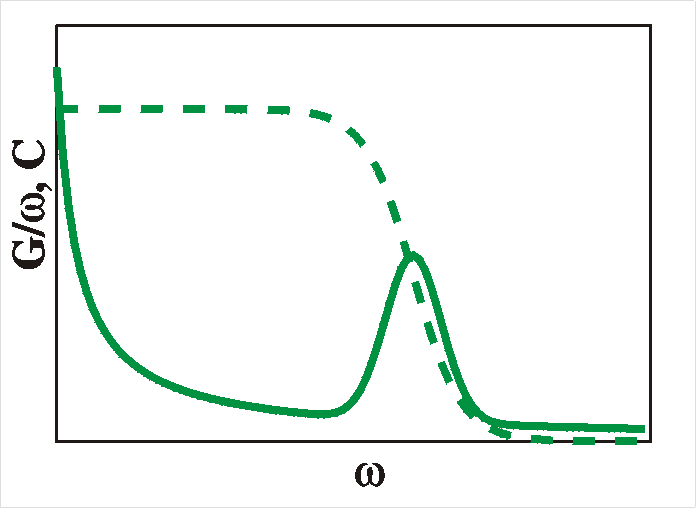
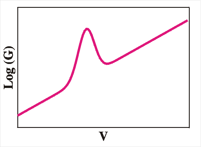
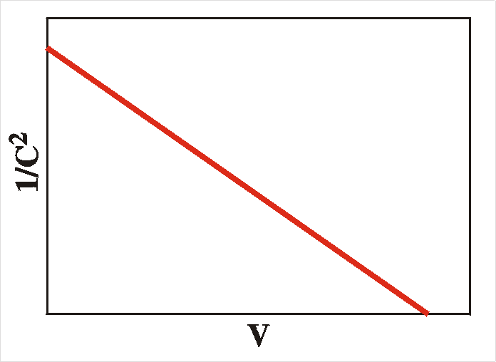
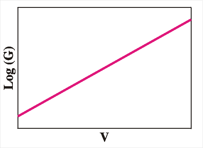
well as a peak in conductance-voltage (GV), see the figure below.
 |
 |
|
C-2-V
plot (left) and Log(G)-V plots (right) when interface
states are present
|
As for the frequency response, this is identical to the deep states:
For very low frequencies the interface states have adequate time to
reach thermal equilibrium at all moments and the amount of charge
transferred is proportional to the number of interface states and is
independent of the frequency. When the frequency is increased beyond
the relaxation time of the levels (see section on emission
and capture of carriers) the amount of charge transferred is
diminished, simply because the levels have no time to reach thermal
equilibrium. We will measure a much reduced capacitance and
conductance.
As a secondary effect, even when the interface states are not
responding, they still change the CV plot. this is because charged
interface states contribute to the space charge and this means that
the depletion width shrinks and the capacitance increases. (Note:
technically speaking this only happens when the levels are present
in a non-infinitesimally thin region dW. Otherwise, if they
are truly in a delta function at the interface they do not
contribute to the voltage drop which is the double integral of the
space charge). This is very similar to non-responding deep states
from the previous section; even if the states are not responding,
they still contribute the capacitance.
To summarize: for interface states we expect a peaked response in
the CV and GV plots and flat Cw and Gw plots up to a certain frequency from
where they will fall off rapidly. A maximum in loss-tangent (tand = G/wC)
occurs when the radial frequency w is
equal to the reciprocal relaxation time 1/t.
continuous band of states
If, instead of a nice well-defined bunch of interface states - or,
even better, a single interface state level as described above - we
have a continuous band of states in the forbidden gap of the
semiconductor, we can still do the measurements. For every ac
frequency we get different CV and GV plots. The states that respond
best to the probing are the ones with trap-filling-and-emptying
times in the order of the ac modulation period.
With the bias we can select which states we will measure (see Fig. 1
of this section). These states have a certain relaxation time (t). The deeper the level, the longer the
relaxation time: t = exp(-Et/kT).
If we now measure the loss as a function of the ac frequency we can
expect a peak when the frequency hits the reciprocal relaxation
time, wmax = 1/t. Then, if we increase the bias, this peak
will move to higher frequencies. Such a movement is then immediately
a proof that we are measuring interface states and not bulk states
(Stallinga, 2001 ).
Note
that the relaxation time of bulk states is independent of where (in
space) the Fermi level crosses these levels and hence
independent of the bias.
Summary of CV and GV measurements
Above we have shown how the simple picture of shallow levels
resulting in a straight-line C-2V
plot is distorted by the presence of deep levels or interface
states. The table below summarizes the CV and GV measurements for
Schottky barriers and p-n junctions
|
model
|
C-2-V
plot
|
Log(G)-V plot
|
spectra
C, G/w
and
tand
|
E: single shallow level
x: homogeneous |
straight line
|
straight line
|
"flat" (1/w)
|
E: + deep levels
x: homogeneous |
+ bend or drop
|
straight line
|
peak
|
E: + deep levels
x: interface (or local)
states |
+ peak
|
peak
|
peak (only at certain voltages)
|
E: + deep levels,
homogeneously
distributed
x: interface (or local)
states |
peak (pos. depending
on ac frequency) |
peak (pos. depending
on ac frequency) |
peak (pos. depending on bias) |
Admittance spectroscopy, equivalent
circuits
As we have seen above, the values of the measured capacitance (C)
and conductance (G=1/R) depend on the probing
frequency. The determination of this dependence, i.e., the
shape of the spectra, is called admittance spectroscopy.
Very often, the data can be described very well with
equivalent circuits. The advantage of them is that a lot of things
can be described in this way, but the disadvantage is that the
physical meaning of the found parameters is often difficult to
interpret. One example of an equivalent circuit that is very
illustrative and that still has a strong link with the actual
physical structure of the device is the following:
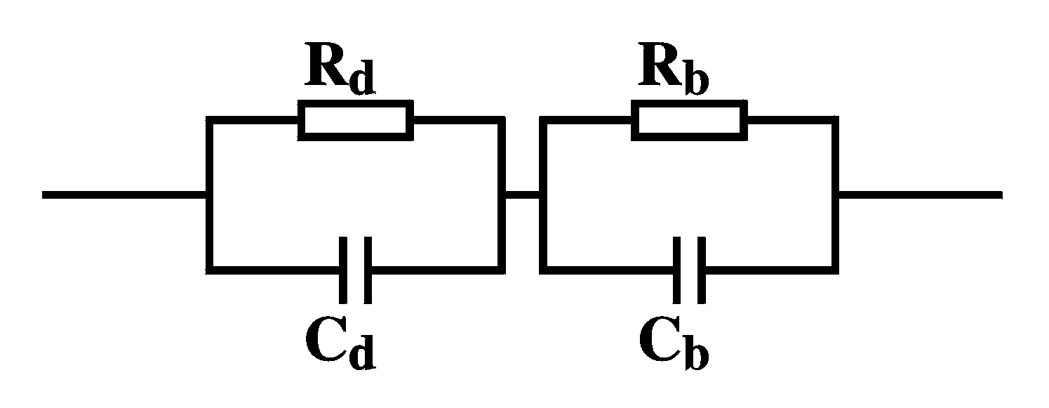 |
In the picture on the left the device is thought of as
consisting of a bulk part (denoted with b) with its
capacitance and resistance placed in series with the
interface part (denoted with d). |
This seems a very reasonable assumption. Even in such a simple
circuit, the measured capacitance and conductance follow
complicated equations. Even if we take the elements in the circuit
to be frequency independent, the measured values are not. Some
calculations can show that
| C = |
Rd2Cd
+ Rb2Cb
+ w2Rd2Rb2CdCb(Cd+Cb)
|
 |
|
(Rd+Rb)2
+ w2Rd2Rb2(Cd+Cb)2
|
| G = |
Rd + Rb + w2RdRb(RdCd2+RbCb2)
|
 |
|
(Rd+Rb)2
+ w2Rd2Rb2(Cd+Cb)2
|
Under the approximations Rb << Rd
and wRbRdCd2
>> 1 the loss tangent reduces to
| tand
= |
wCdRb
|
 |
|
1 + (wRb)2(Cd+Cb)Cb
|
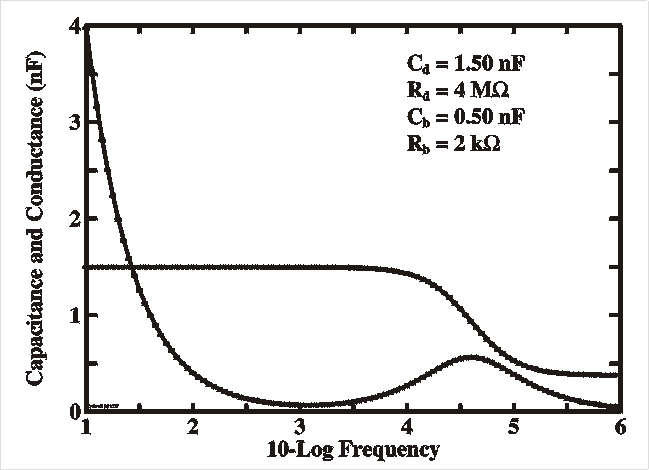
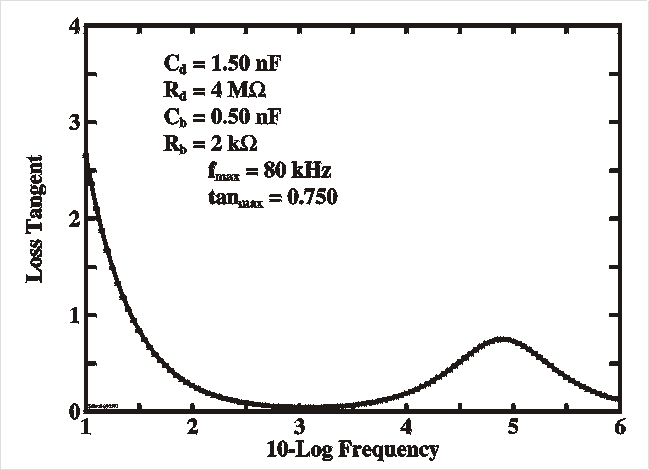
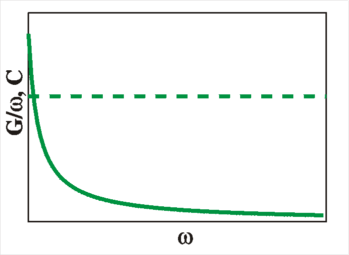
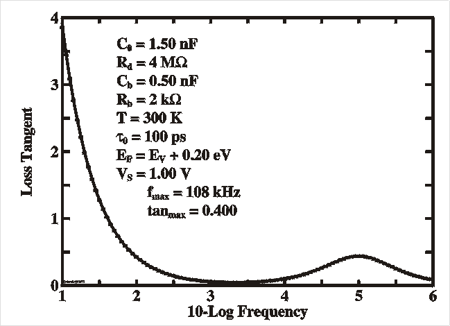
| The Figures show a simulation of the capacitance and loss
(G/w) (left) and loss
tangent (right) as a function of the probing frequency n (=w/2p) with the parameters as given in
the Table. This resembles very much the spectra of deep
levels and interface states as described in the previous
sections. It is clear that for low frequencies the
capacitance flattens out and saturates at the interface
value Cd (assuming this is the larger of
the two), while for higher frequencies it reaches the bulk
value. This bulk value is in fact the so-called geometrical
capacitance Cgeo which is the capacitance
of the parallel plates with area A at mutual
distance d filled with a dielectric medium e. |
|
param.
|
value
|
| Cd |
1.50 nF |
| Rd |
4 MW |
| Cb |
0.50 nF |
| Rb |
2 kW |
|
|
w=0
|
w=oo
|
w=wmax
|
| C |
Cd
|
Cb
|
|
| R |
Rd
|
Rb
|
|
| tand |
1/wRdCd
|
1/wCbRb
|
Cd/2(Cb(Cb+Cd))1/2
|
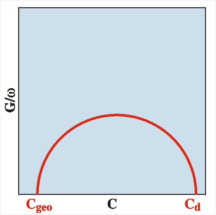
| Some people prefer to present the admittance data in the
form of so-called Cole-Cole plots. In that case we plot the
loss versus the capacitance. The figure shows an example.
For systems as described above it can be shown that the plot
is a semicircle (with the center on the horizontal axis) and
meeting the horizontal axis at C=Cgeo
and C=Cd. If we know the
dimensions of the device, A and d, we can
calculate the permittivity e of
the material:
e = dCgeo/A
|
 |
In the figures of the loss-tangent we see a local maximum
somewhere at a frequency
 This gives a handle for the measurement of the
activation energy of the bulk conductance. When the temperature is
changed, the bulk resistance changes and - assuming that the
capacitances are relatively independent of temperature - the
position of wmax should
follow the bulk resistance. With the assumption that the bulk
conductance is singly activated, the resulting temperature
dependence of wmax is
This gives a handle for the measurement of the
activation energy of the bulk conductance. When the temperature is
changed, the bulk resistance changes and - assuming that the
capacitances are relatively independent of temperature - the
position of wmax should
follow the bulk resistance. With the assumption that the bulk
conductance is singly activated, the resulting temperature
dependence of wmax is
wmax = w0 exp(-Eb/kT)
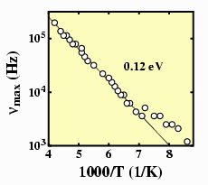
Hence, an Arrhenius plot of the position of the peak in the
loss-tangent graph, log(wmax)
vs. 1/T, will yield the bulk activation energy Eb.
The Figure gives an example for an MEH-PPV device (P. Stallinga et
al., submitted to J. Appl. Phys., 1999 )
In the above theory, all parameters are assumed constants. This
is not a correct picture. For instance, the capacitance of the
depletion layer Cd is temperature and frequency
dependent. A distribution of levels in energy will cause a
frequency dependent capacitance of the form
| Cd = C0 |
 |
1 - |
kT
|
log |
|
1 + w2t02 exp[ 2
(EV - EF
+ qVS)/ kT]
|
 |
|
|

|
|
2qVS
|
1 + w2t02 exp[ 2
(EV - EF)/
kT]
|
For w=0 Cd reaches
the low frequency value C0 (which is still
voltage dependent), while for infinite frequencies the capacitance
drops to zero. For deep levels, with t
very slow, the most visible result is that the capacitance doesn't
flatten out at lower frequencies. Otherwise not much changes. The
position of the maximum of the loss tangent, for instance, is
rather invariant to such effects.
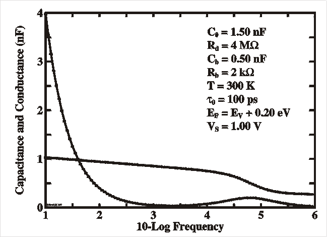
| param. |
value
|
|
param. |
value |
| C0 |
1.50 nF |
|
T |
300 K |
| Rd |
4 MW |
|
t0 |
100 ps |
| Cb |
0.50 nF |
|
EF-EV |
0.2 eV |
| Rb |
2 kW |
|
VS |
1 V |
The Figures show a simulation with the same parameters as before
but now with a frequency dependent capacitance. Note the
non-saturating capacitance at lower frequencies.
Some remarks:
- The equivalent circuit can be expanded with other RC loops.
For instance, an extra RC loop can be added to simulate that the
material has two parts with different doping densities
(see Forero et al., 1999 ). Every loop
causes a peak in the loss-tangent and an extra semi-circle in
the Cole-Cole plots. Therefore, if we have n loops, we
will have n-1
semicircles and n-1
peaks in the loss-tangent.
Also loops can be added that do not directly have a link to the
geometrical nature of the device. In principle any process
that has a relaxation time t can be
simulated with a loop, such that t = RC.
For example the relaxation process from the interface states as described in the
previous section. Via the temperature dependence of the peak in
the loss tangent, and hence of the time constant t, the activation energy of this process
can be measured. The physical meaning of the equivalent circuit is
then lost, but the electronic engineer still likes to model the
device in circuits.
Measuring mobility
The (drift) mobility of the carriers is defined as the ratio of
carrier velocity v and electric field E:
v = mE
That is, if we had any way of directly measuring the velocity of our
carriers, assuming we know the electric field, we could directly
find the mobility. In reality, measuring the velocity is difficult
and we have to resort to more indirect methods.
To measure the mobility we have many tools to our disposal. The
following sections describe the most common: Field-Effect
Transistor (FET), Hall, Time of Flight
(ToF). In some cases it is also possible to measure the mobility
directly from an ohmic sample. For organic semiconductors the most
common technique is via FETs. This is because it is a rather simple
and cheap method. Moreover, the rather low mobilities of the
carriers in organic materials make measuring in a Hall set up
difficult. Since the results of the various measurements can be
varying tremendously, we always have to specify wit which method the
mobility was measured. Therefore, there exist mFET,
mHall, mToF,
etc.
Field Effect Transistor
(See also special pages on FETs
for more detail)
A field effect transistor (FET) is worth to mention here because we
can get additional information about the material. An FET is a
structure in which the material under study is deposited on top of
oxidized silicon. The silicon substrate is low ohmic and acts as the
gate. On top of the polymer layer metal electrodes (source and
drain) are deposited in a pattern with small inter-electrode
distance. The voltage on the gate now controls the current through
the source-drain channel. It either stimulates it (in an enhancement
FET) or decreases it (in a depletion FET). In either case, we can
determine the carrier mobility m from
the data.
 |
| symbol |
meaning |
| L |
channel length |
| Z |
channel width |
| d |
oxide thickness |
| VG |
gate voltage |
| VD |
drain voltage
(VS=0) |
| ID |
drain current |
| m |
(hole) mobility |
|
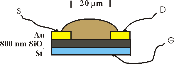
| MOSFET (Metal Oxide Semiconductor
Field Effect
Transistor) structure. In
this case the metal is replaced by low-resistive
silicon. The current from source (S) to drain (D) is
controlled by the gate (G) voltage |
The source-drain current, ID follows the equation
ID = (Z/L) m
Ci [(VG-VT)VD-aVD2]
or for small VD:
LIN:
ID = (Z/L) m Ci
[(VG-VT)VD]
The saturation current follows the equation
SAT: IDSAT
= (m Z/L) mCi
(VG-VT)2
with m =1/2 for light doping (see p. 442 of Sze ). L
is the channel length (distance between source and drain), Z
is the channel width (length of source or drain electrode). The
insulator thickness (d) or source-gate or drain-gate distance
enters into the equation via the oxide capacitance Ci
= e/d (capacitance per unit
area), which can either be measured or calculated. For example,
silicon oxide has an er of
3.9, with a d of 8000 Angstrom this gives Ci =
43.2 10-6 F/m2.
Here is an example: The picture on the right shows the IV plots (ID
vs. VSD) of an FET for various gate-source
voltages (VS=0), ranging from 0 V (top) to -35 V (bottom) in steps of 5 V. With a
source (and drain) electrode length of 25 cm and distance of 25 mm and oxide thickness of 800 nm the
mobility of the holes can be calculated to be 3 10-6 cm2/Vs.
Effects that we have to be aware of are
Velocity saturation. For high fields, the velocity of the
carriers is not proportional to the field, but instead saturates
to a certain value. This makes that the saturation current (Ids
for Vds > Vgs-Vt) depends linearly on
the gate voltage rather than quadratic (see p. 450 of Sze, )
Contact resistance. If we ignore the contact (or series)
resistance at the electrodes of the device, we can underestimate
the mobility, see Horowitz et al, JAP 1999).
Short-channel effects. These occur when the inter-electrode
distance becomes comparable to the depletion layer widths. In this
case, all sorts of deviations from standard theory can occur, see
section 8.4 of Sze .
Other non-linear effects can make the mobility (gate)
voltage dependent. In most cases the mobility drops for increased
gate-voltage (Fig. 8.13 of Sze, ), but also the
opposite can happen (Vissenberg, PRB 1998, ).
A good starting point for measuring organic FETs is the article
of Horowitz, "Organic Field-Effect Transistors" .
Hall measurements
When we take a bar of semiconductor without any rectifying
contacts we can measure its resistivity r,
or conductivity s=1/r which can be
expressed in terms of mobility and free-carrier density:
s = e mpp
(e is elementary charge, mp
is hole mobility, p is hole density). In a Hall experiment
we can simultaneously measure the product ep and therefore
we can determine the mobility of the carriers. This works as
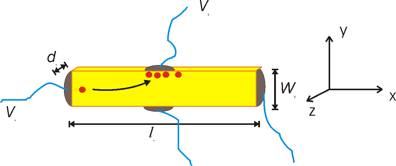
follows. A voltage is applied along the x-direction and the
conductivity is measured:
s = (Ix / Vx)
(lx / Wydz)
mp = (Ix
/ Vx) (lx / Wydz)
/ ep
Eq.1
with Ix the current, Vx the
voltage, lx the sample length, Wy
the sample width and dz the sample thickness. At
the same moment a magnetic field is applied along the z-axis. This
creates a Lorentz force on the moving holes
FyB = e Bzvx
with Bz the magnetic field strength and vx
the drift velocity of the holes. Holes will therefore move to the
edge of the sample where the built-up of this charge will create an
electric field that will compensate the magnetic forces
FyE = -eEy
At steady state the two forces are equal
Bzvx = Ey
The electric field Ey can be determined by
measuring the voltage Vy on the sides of the bar
and dividing by the sample width Wy. If we
further realize that the velocity of the holes is equal to Jx/ep
= Ix / (Wydzep)
we can express the above equation as
Bz Ix / (Wydzep)
= Vy/Wy
ep = Bz Ix / Vydz
If we apply this to Equation 1 we find that in a single experiment
we can determine mp:
| mp |
= |
lxVy
|
|
|
BzVxWy
|
The mobility measured in this way is the so-called
Hall-mobility. It can deviate from the mobilities measured in
other experiments. For instance, the assumption is made that all
holes move with the same velocity vx. This is, in
fact, not true. A Boltzmann distribution is a much better
approximation. Such effects are normally accounted for in a
correction factor r, which will not be discussed here. The
factor lies in the range 1-2. See Chapter 3.2 of Blood and
Orton .
Note that the sign of the voltage Vy depends on
the type of the carriers. In this way we can unambiguously determine
if the semiconductor is p-type or n-type.
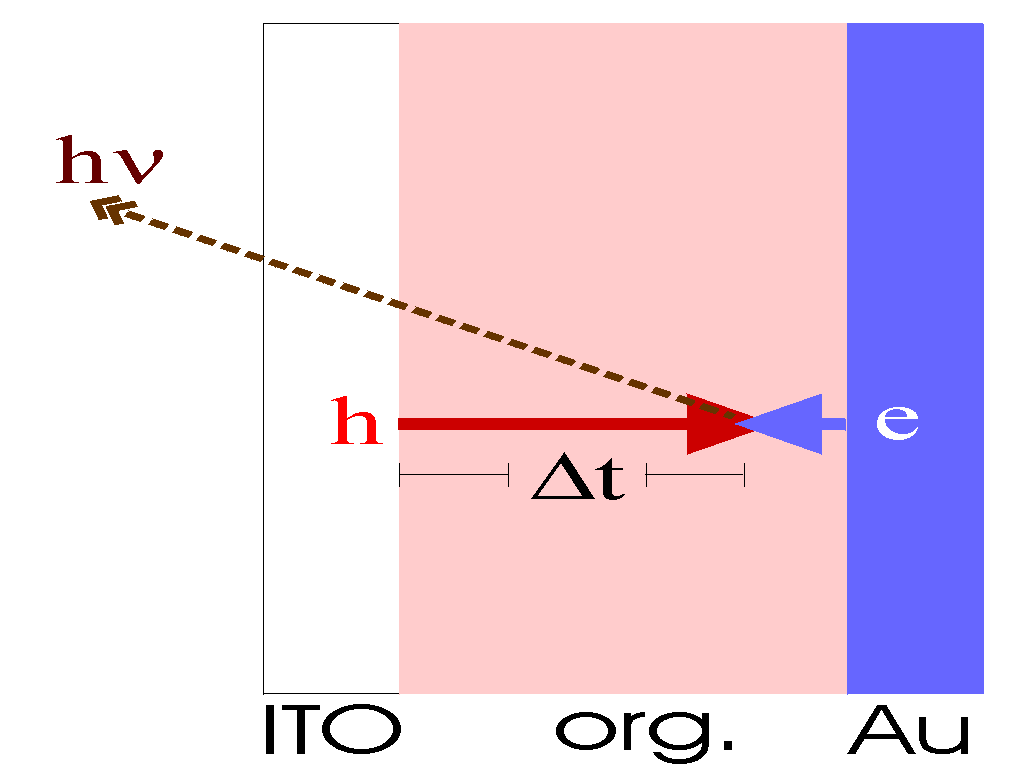
Time-resolved
Electroluminescence
| This method is probably the most direct way of measuring
the velocity and hence the mobility of the carriers. With an
electric pulse, electrons and holes are injected from
opposite sides into the active layer. When the carriers
meet, somewhere in the active layer, they will recombine and
produce light. The time delay (Dt)
to the onset of luminescence directly gives you the speed of
the fastest carriers (in most organic materials these are
holes), assuming you know the thickness of the layer (d)
through which the carriers must travel
m = v/E = (d/Dt) / (V/d)
= d2 / VDt
|
 |
Time of Flight (ToF)
This method is similar to time resolved electroluminescence, but
instead of measuring the light we measure the time-resolved
current on the other side of the voltage or light pulse. The
results are the same.
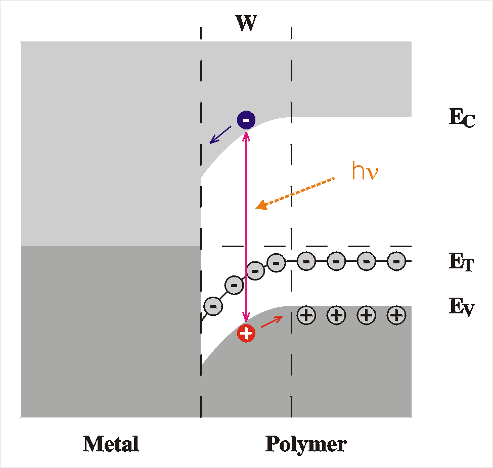
Optical effects
Wherever there is a rectifying contact (be it a Schottky barrier or
a hetero-junction) we can expect strong optical effects. The
device can either be used as a photo-detector or an LED
(light-emitting diode). The underlying mechanism is the same
in both cases, namely the depletion zone which is void of free
carriers in thermal equilibrium and has (for the same reason) a
strong electrical field. Let us first look at the reason why a
rectifying contact can emit light:
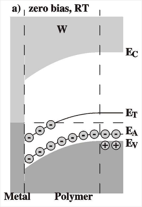
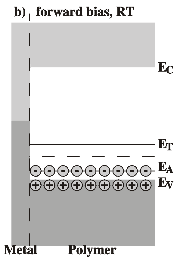
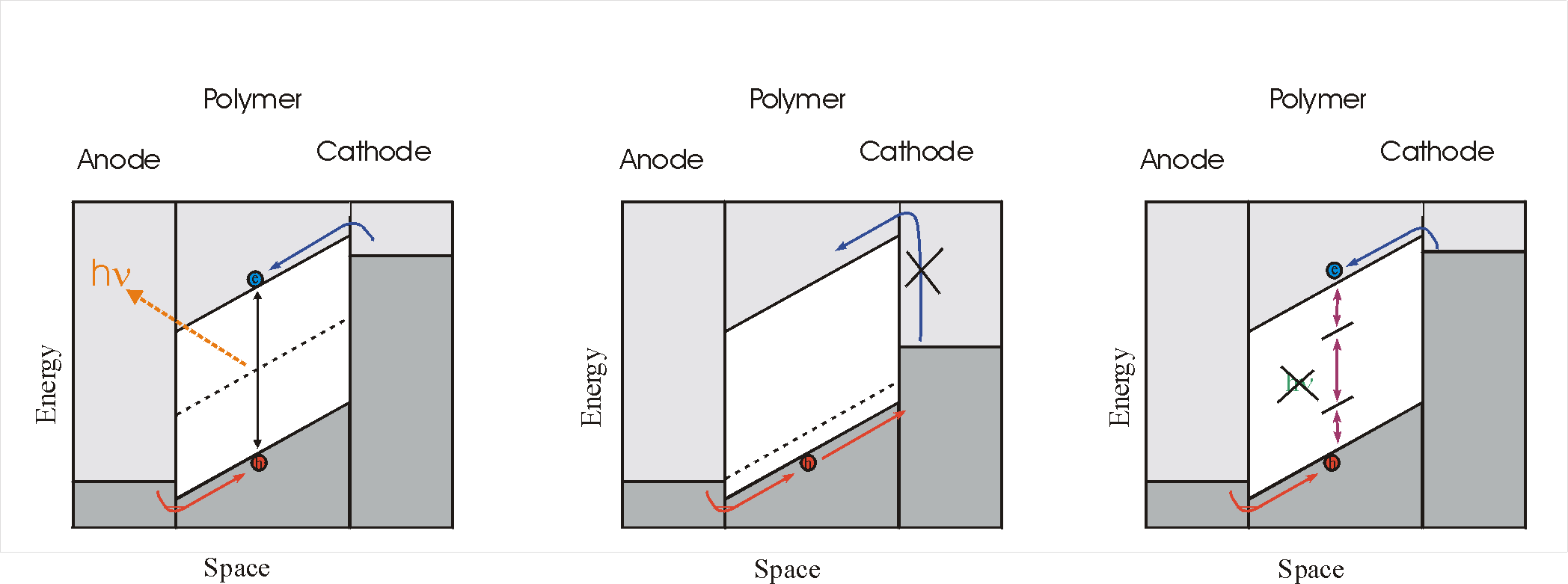
Light emitting diode:
Under forward bias, majority carriers (holes from the polymer and
electrons from the metal) are injected into the depletion region.
As the name implies, and as we have seen in the beginning of this
document, in thermal equilibrium density of free carriers in this
region is very low. The injected carriers will therefore try
to recombine in a constant way restoring equilibrium. The energy
that is released in the process is carried of in the form of
photons, which, if they are not reabsorbed in the material can be
detected externally.
The energy of the photons, and hence their wavelength (read color)
is determined by the difference in energy between the holes and
the electrons. Holes are mostly available in the top of the
valence band and electrons in the bottom of the conduction band.
This energy difference is therefore equal to the bandgap. For
classical semiconductors (e.g. Si) this energy is in the range of
infra-red. For wide bandgap semiconductors (such as GaN and
most polymers) the bandgap is in the order of 2.5 eV and this
implies that the photons are in the blue part of the spectrum. A
decade ago, the existence of blue LEDs was still a thing of the
future and research was focused on finding a suitable material.
Candidates included SiC, GaN, ZnSe, etc.
In the ideal case, all injected electrons recombine with all
injected holes (somewhere in the middle of the depletion region)
and the quantum efficiency is then 1, namely one photon emitted
for every electron-hole pair injected.
It has to be noted that for an LED it is not necessary that there
exists a rectifying contact. The only prerequisite is a region of
low equilibrium-free-carrier concentration into which free
carriers are injected. In fact, most polymer LEDs are made
of ultra-pure (and hence highly depleted) semiconductor material
sandwiched between two metals (often transparent ITO, indium-tin
oxide) which act as electron injectors (cathodes) and hole
injectors (anodes). Because there is no space charge inside
the polymer there exists a linear voltage drop, instead of the
quadratic voltage drop of Schottky barriers, see the figures
below.
There are two ways the light efficiency might be impaired:
- Unbalanced carriers. If only one of the types of free
carriers are injected into the depletion region, there is
obviously no recombination. In that case, the excess
energy is carried off in the form of heat.
- Non-radiative recombination. If there exist
recombination paths without the emission of photons, the light
efficiency can also be reduced. Many defects are non-radiative
recombination centers. In a way, defects are needed to provide
the material with free carriers in the neutral regions, but in
another way, defects are unwanted because they can reduce the
luminescent efficiency. On the other hand, for fast, non-optical
electronics, recombination centers are needed
|
a working LED
|
an LED hindered by un-
balanced injected carriers
|
an LED limited by non-
radiative recombination paths
|
Photo-detector / solar cell:
| In a photo-detector or solar cell, the opposite process
takes place. The energy of photons is used in
producing electron-hole pairs which are subsequently
broken up by the strong electrical field in the interface.
These free carriers arrive at the electrodes where they
contribute to an external current. In this case, it is
also not really necessary that there exists a rectifying
contact. The only prerequisite is a strong electric field
at the place where the electron-hole pair are formed. This
field should be stronger than the binding energy of the
e-h pair. At Schottky barriers such fields are easily
present because the voltage drop occors over a very small
length, but at sandwich structures large external voltages
are needed. Moreover, no short-circuit currents are
possible; The moment we short-circuit the device, the
field is (nearly) gone and carriers are not separated or
transported to the electrodes. Thus, while the sandwich
structures are still good for photodetectors, they are not
suitable for solar cells. |
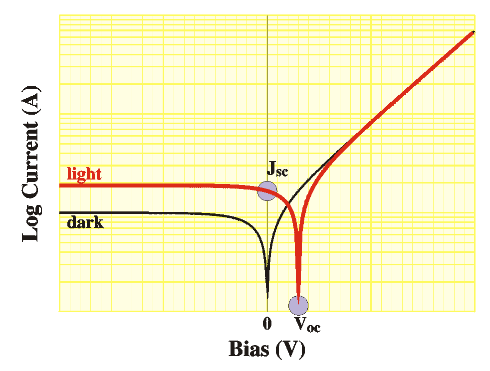
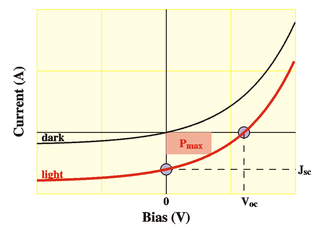
The parameters that characterize a solar cell are
- the open-circuit voltage (Voc). This is the
voltage when no current is running and in the IV-plot this is
the voltage where the IV curve intersects the voltage axis.
- the short-circuit current (Jsc). This is the
current when no voltage exists across the device and in the
IV-plot this is the current where the IV curve intersects the
current axis.
The value for Voc is always positive and the
value of Jsc is always negative; the current
resembles a reverse-bias current.
The product of J and V has a minimum
somewhere. This is the maximum power Pmax
that the solar cell can generate.
The figures show the IV curves in the dark (black) and under
illumination (red) in logarithmic scale and in linear scale.
Emission and capture of carriers
For all the transient techniques of monitoring a system parameter
over time we bring the system off-equilibrium in some way and
observe how fast it recovers to thermal equilibrium. The
bottleneck process is in most cases the emission and capture of
carriers on deep levels, although in some rare cases it is the
diffusion of the free carriers out of the depletion zone. This
section describes the relaxation process of reaching thermal
equilibrium in the deep states.
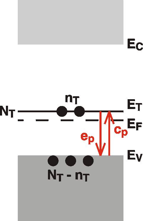 The
Figure shows the processes of capture and emission of holes from a
deep acceptor level at ET with density NT.
The number nT stands for the number of levels
filled (with holes). The rest of the holes, NT-nT, must then be in the
valence band (in this simple model which neglects a contribution
of the intrinsic holes originating from the conduction band). The
other numbers, ep and cp
stand for the emission and capture rates (in units
number-per-second-per-available-hole). The number of holes
actually being emitted and captured is then proportional to these
values and the number of available holes in the states: cp(NT-nT) holes per second
will be captured onto the trap and epnT
will be emitted per second. In equilibrium there is no net
transfer of holes. This requires
The
Figure shows the processes of capture and emission of holes from a
deep acceptor level at ET with density NT.
The number nT stands for the number of levels
filled (with holes). The rest of the holes, NT-nT, must then be in the
valence band (in this simple model which neglects a contribution
of the intrinsic holes originating from the conduction band). The
other numbers, ep and cp
stand for the emission and capture rates (in units
number-per-second-per-available-hole). The number of holes
actually being emitted and captured is then proportional to these
values and the number of available holes in the states: cp(NT-nT) holes per second
will be captured onto the trap and epnT
will be emitted per second. In equilibrium there is no net
transfer of holes. This requires
epnT = cp(NT-nT) Eq.1
The holes must also obey the Fermi-Dirac distribution (note that
this is the distribution for holes! Levels are full when they are above
the Fermi level):
nT / NT =1 / [1 +
exp{(EF-ET)/kT}]
Eq.2
and therefore we can calculate the ratio of emission and capture:
ep / cp = exp{(EF-ET)/kT}
Eq.3
To verify if this is correct: imagine a situation with the trap far
below the Fermi level. In that case, the above equation tells us
that the emission rate is much larger than the capture rate and the
levels will be empty (contain no holes). This is exactly what we
expected on basis of the starting assumption of the position of the
Fermi level.
As seen above, the ratio of emission and capture depends on the
Fermi level. We now make the assumption that the emission of holes
from a trap level to the valence band is a property of the trap1.
The capture of holes from the valence band is proportional to 1:
the capture cross-section, sp.
2: the number of free holes in the valence band, p. 3: the
average thermal velocity of these free holes, <vp>.
In
Equation 1:
cp(NT-nT)
=
sp <vp>
p
Also we know that the density of free holes is governed by the Fermi
level:
(NT-nT)
= p = NV exp{-(EF-EV)/kT}
Further we need an approximation that most of the trap levels are
empty. Equation 2 then becomes
nT = NT exp{(ET-EF)/kT}
And with these three terms, the emission rate of Equation 1
becomes:
ep = sp
<vth> NVexp{-(EF-EV)/kT}/
NT exp{(ET-EF)/kT}
= sp <vth>
[NV / NT] exp{-(ET-EV)/kT}
If we substitute the absolute expressions for the parameters
sp = s0 exp[ -DEs/kT ]
<vp> = [3kT / m*]1/2
NV = 2MV [ (2pm*kT)/(h2)
]3/2
we can calculate the explicit temperature dependence of the emission
rate
ep = gT2spa
exp(-Epa/kT)
This defines the pre-factors g and spa, which are not so interesting
for the experiment. On the other hand, a plot of ln(ep/T
2) vs. 1/T will show a straight line and
reveals the activation energyEpa of the
trap. In the case when there is no capture (for instance when
all the free holes are immediately swept away by the electric
field), the thermalization time constant is equal to the reciprocal
of ep and can be measured in the experiment. This
gives a possibility of determining the trap activation energy
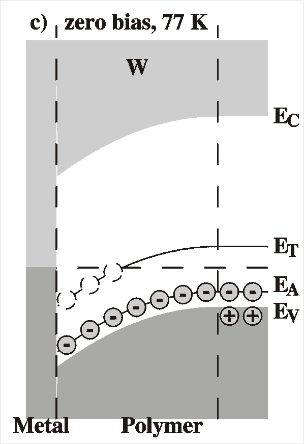
directly, as we will see later in the section on DLTS.
1: we make here the assumption that the number of
available "destination" states is infinite so that is not
causing a bottleneck in the emission process
Capacitance-Transient spectroscopy
(predecessor of DLTS)
In DLTS (deep level transient spectroscopy) the capacitance is
monitored over time after a sudden change of bias. The above
figures clarify what happens to the capacitance after a switch of
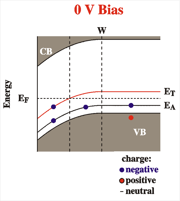
bias. Easiest is it to understand if we remember that the
capacitance is directly linked to the depletion width:
C = Ae/W
So, if for instance for some reason the depletion width increases,
the capacitance decreases.
Assume that the device is completely in thermal equilibrium at 0 V
bias (left Figure). All the levels, even the deep ones, have their
thermal equilibrium populations and a certain depletion width and
capacitance is attained. (See the section on Calculation
of the depletion width if you want to read again how to find
the depletion width via double integration of Poisson's Equation d2V/dx2
= r). The depletion width W is
determined by
 r(x)d2x
= Vbb
The integration is done from x=W to x=0. Vbb
is the total band bending or voltage drop, Vbb =
Vbi-V. Note that
in the above Figures, the charge density is not constant; inside the
depletion width there exists a smaller region where the deep level
is below the Fermi level and where the space charge is larger.
r(x)d2x
= Vbb
The integration is done from x=W to x=0. Vbb
is the total band bending or voltage drop, Vbb =
Vbi-V. Note that
in the above Figures, the charge density is not constant; inside the
depletion width there exists a smaller region where the deep level
is below the Fermi level and where the space charge is larger.
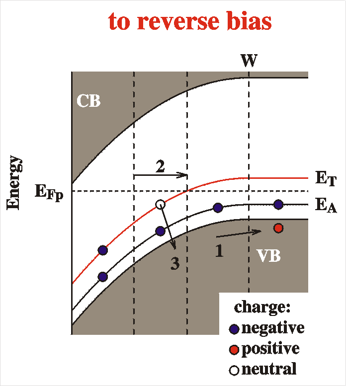
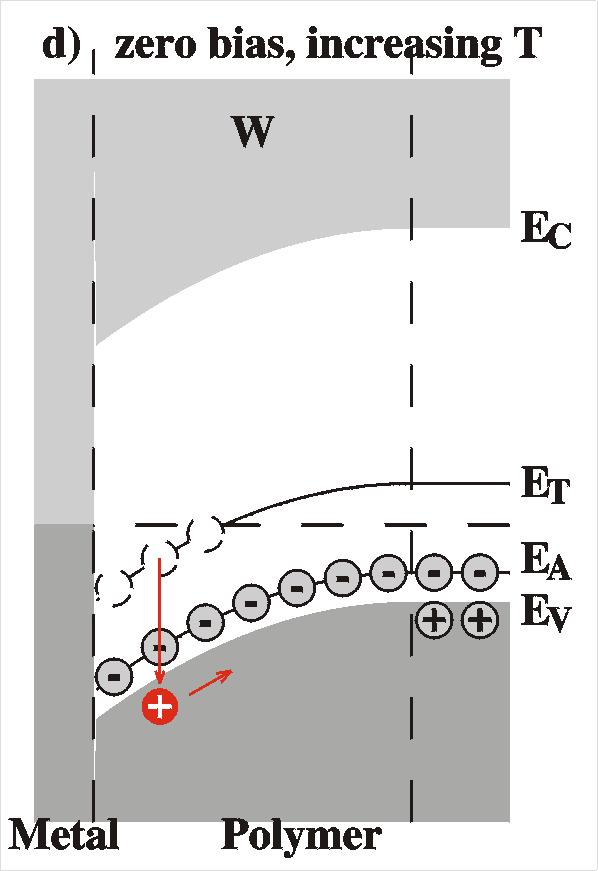
When the voltage is switched to reverse bias many things will
happen. A different voltage drop Vbb occurs at
the interface. This implies a new depletion width and a new
capacitance according to the above equations. The new equilibrium
capacitance takes time to reach. The following things will happen:
- 1: The free carriers (holes in the valence band) will rapidly
move out of the interface region. The space charge increases.
- 2: A new, larger, depletion width is reached.
- Larger depletion width means smaller capacitance.
- Inside the new depletion width the deep level, which cannot
respond so fast, is off equilibrium close to the interface.
- 3: Charges (holes) are slowly emitted from the deep level to
the valence band at a time scale t.
These charges are immediately swept away by the electric field.
- Because the space charge density increases closer to the
interface, less depletion width is needed. (Visualize: the
integration of Poisson's Equation reaches Vbb
a little earlier). W shrinks.
- If W shrinks, C increases. This then happens
at a time scale of the hole emission life time t.
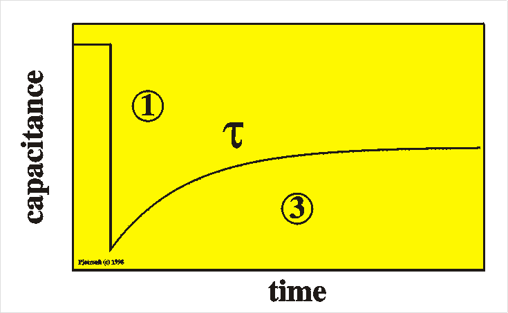 To summarize: after a switch of the voltage to
reverse bias we first observe an immediate decrease of the
capacitance (1) and after that a slow (partly) recovery of the
capacitance at time scale t (3). The
explicit form of the time dependence of the capacitance is
C(t) = C0 + DCexp[-t/t]
To summarize: after a switch of the voltage to
reverse bias we first observe an immediate decrease of the
capacitance (1) and after that a slow (partly) recovery of the
capacitance at time scale t (3). The
explicit form of the time dependence of the capacitance is
C(t) = C0 + DCexp[-t/t]
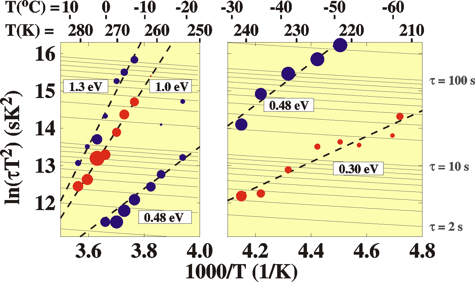
To find the trap activation energy, Epa, we
can use the equation for the emission rate ep
(=1/t) found in the section Emission and capture of carriers. ep
= gT2spa exp(-Epa/kT).
If we monitor the characteristic decay times of the transients as
a function of temperature and plot this in the form ln(tT 2) vs. 1000/T,
the resulting straight line will yield the activation energy.
Note: to truly measure the capacitance of the interface, Cd,
we must chose a frequency low enough to be below the cut-off
frequency of the bulk, see the section on admittance
spectroscopy. For higher frequencies we would measure only
the bulk properties, which have no transient effects.
capacitance transient of minority
traps
 For minority traps the idea is similar. We have to keep in mind,
though, that a minority trap is a trap that more readily
communicates with the minority-carrier band than with the majority
carrier band. For instance, an electron trap will thermalize with
the conduction band rather than the valence band as described in the
previous section. In other words, we have to draw the picture
with the minority quasi Fermi level EFn
rather than the majority quasi Fermi level EFp.
As explained before, the minority quasi Fermi level moves in the
opposite direction compared to the majority quasi Fermi level.
For minority traps the idea is similar. We have to keep in mind,
though, that a minority trap is a trap that more readily
communicates with the minority-carrier band than with the majority
carrier band. For instance, an electron trap will thermalize with
the conduction band rather than the valence band as described in the
previous section. In other words, we have to draw the picture
with the minority quasi Fermi level EFn
rather than the majority quasi Fermi level EFp.
As explained before, the minority quasi Fermi level moves in the
opposite direction compared to the majority quasi Fermi level.
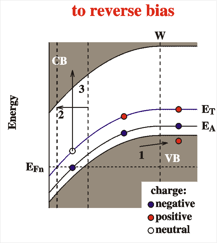
When the voltage is switched to reverse bias, the following
things happen (the differences for minority carrier traps are
indicated in a bold font):
- 1: The free carriers (holes in the valence band) will rapidly
move out of the interface region. The space charge increases.
- 2: A new, larger, depletion width is reached.
- Larger depletion width means smaller capacitance.
- Inside the new depletion width the deep level, which cannot
respond so fast, is off equilibrium close to the interface.
- 3: Charges (electrons) are slowly emitted from the deep
level to the conduction band at a time scale t. These charges are immediately swept
away by the electric field.
- Because the space charge density decreases closer to
the interface, more depletion width is needed.
(Visualize: the integration of Poisson's Equation reaches Vbb
a little later). W increases.
- If W increases, C decreases.
This then happens at a time scale of the hole emission life time
t.
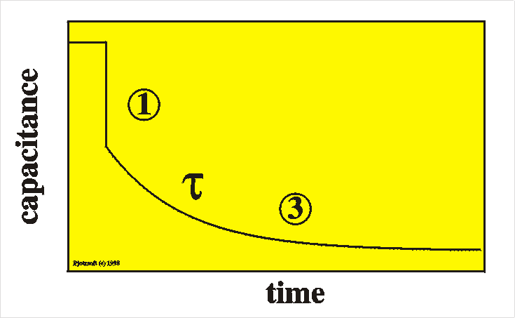 |
To summarize: after a switch of the voltage to reverse
bias we first observe an immediate decrease of the
capacitance (1) and after that a slow further decrease of
the capacitance at time scale t (3).
This is very similar to majority carrier traps, but the sign
of the transient is reversed; DC
is positive here. We can still determine the trap activation
energy by monitoring the characteristic transient decay time
t as a function of temperature. |
As an example the following graph of energy levels in MEH-PPV on
silicon substrates as determined by capacitance-transient
spectroscopy (taken from P. Stallinga et al., Synthetic
Metals 1999; see reference list). The blue dots are majority-carrier
traps with upward-trend transients and the red dots are
minority-carrier traps with downward-trend transients. The size of a
dot represents the transient amplitude (in the right panel it is
multiplied by 5 for better visibility). The plot reveals several
trap levels and shows the result of the first successful capacitance
transient experiment in MEH-PPV.
DLTS (deep level transient spectroscopy1)
Historical background
Deep level transient spectroscopy is probably the most used
technique in the electrical characterization of semiconductors. This
is based on the fact that it is fast, cheap in terms of equipment,
and very sensitive. Commercially sold set ups exist in abundance.
The inventor of DLTS is D.V. Lang who wrote an article how to
analyze capacitance transients in a systematic way , at
that time enabled by the advent of modern computers with their
data-crunching and experiment-steering powers. Looking back at it
now, it can be said that "it was time" for such a technique to be
invented. Lang did it and is now one of the most cited people in
literature. His first article in the Journal of Applied Physics is
still the best source for understanding the technique. Most things
are described very elegantly there. I will do my best to describe it
here.
When the computers became more powerful more modern versions of DLTS
were invented that use more of the data and use more and
more-complicated calculations. The result is an increased resolution
and sensitivity. The Laplace-DLTS technique is a good example. This
uses the entire transient in a Laplace transformation to yield a
much higher resolution. Obviously, for this a lot more calculating
power is needed.
Basic principles
How DLTS works is the following. Capacitance-transients are
recorded in the same way as described above. The device is placed
in the emptying voltage VE and the system is
allowed to reach thermal equilibrium. For a short time the device
is placed under the filling voltage VF. In this
times the traps will fill with charges. When the voltage is
switched back to VE a transient is observed as
described in the previous sections. From this transient two
samples are taken at times t1 and t2
after switching the bias. The DLTS spectrum is now the difference
in capacitance at these two times as a function of temperature:
S(T) = C(t1) -C(t2)
This means (substituting the explicit form of the transient, see
the section on capacitance-transient
spectroscopy)
S(T) = [exp(-t1/t) - exp(-t2/t)]
The maximum of this signal occurs when the relaxation time t reaches the value tmax
which can be found by differentiating S(T) with
respect to t:
tmax = (t2-t1) / [ln(t1/t2)]
The explicit temperature dependence of t
is (see section on emission rates)
t(T) = t0T-2exp(Epa/kT)
From this it is clear that the temperature at which the maximum DLTS
signal occurs does not reveal the activation energy directly, unless
t0 is known. If not, at least
two measurements have to be made with different time windows (t1,
t2) and the two points (Tmax, tmax) entered into the above
equation will yield the trap activation energy Epa.
Parameters of DLTS are:
- Repetition rate: how many times per second a transient is
recorded. The time between two transients should be long enough
to ensure that the system is in thermal equilibrium.
- Time window: The values of the sampling-point times t1
and t2.
- Filling voltage VF and emptying voltage VE.
- Filling time: how long the device is placed in the filling
voltage VF before switching back to reverse
voltage VE.
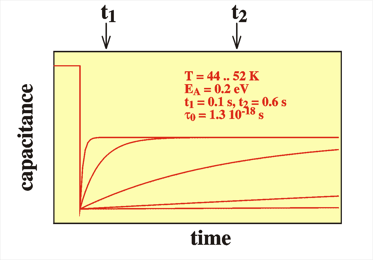 |
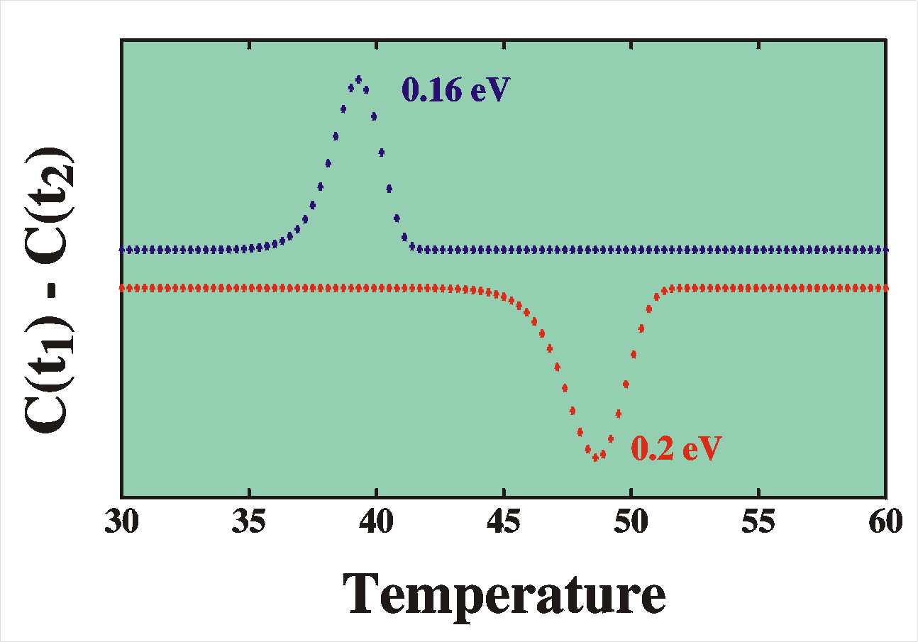 |
| Capacitance transients at several temperatures |
Resulting DLTS signal for majority traps (down)
and minority traps (up) |
Example
The Figures show a simulation of DLTS. The left figure shows
simulations of transients caused by a 0.2 eV deep majority carrier
trap for various temperatures (44 K to 52 K in 2 K steps). For the
lowest temperatures the transients are very slow (bottom trace)
and the difference between the capacitance at t1
and at t2 is small, hence the DLTS signal S(T)
is very small. When the temperature is increased the transients
become faster and the DLTS signal increases. Note that the signal
has negative sign; for majority carrier traps, the transient has
an upward trend and therefore C(t1) is
smaller than C(t2). When the temperature
is further increased, the transients become so fast that they
already died out before the time window (t1-t2)
and the DLTS signal has vanished again. The figure on the right
summarizes this for the majority carrier
trap (red dots; lower trace). In the same figure a
comparison is given with a minority carrier
trap (blue dots; upper trace) whose DLTS signal has the
opposite sign because the related transients have downward trends.
Also, in this simulation the minority-carrier trap is chosen to be
a little more shallow (0.16 eV). Assuming that the pre-factor t0 is identical (1.3 10-18 s in both cases) it means that
the peak has shifted towards lower temperatures.
Comments
The advantage of this scheme is that it can be done completely
automatically with a minimum of data processing. The disadvantage
is that of the entire transient only two points are used; most of
the data are thrown away and the duty cycle of the measurement is
very low. In Laplace DLTS the duty cycle is much higher because
the entire transient is used in a Laplace transformation. The cost
is a more elaborate calculation; only modern computers can be
used.
In reality, DLTS is more often used not to determine the trap
activation energies but more to show the presence of certain
impurities through their fingerprint spectra and to determine
their densities through the intensity of the DLTS spectra and
through the underlying amplitude of the transients. This is based
on the fact that the amplitude of the transient is linearly
proportional to the density of the deep defect relative to the
density of the dopant (assuming that this ratio is small).
DC/C = N /
2(NA-ND)
1: To be precise, the word spectroscopy is
misplaced, because in a spectroscopy experiment an experimental
value is monitored while the frequency is scanned; a spectrum is
the visualization of an observable as a function of frequency.
In DLTS no frequency is scanned, so the name is slightly
inadequate. In DLTS (normally) the temperature is scanned and
the DLTS-signal intensity is plotted. The end plot resembles a
spectrum in that it shows peaks and that it is a "fingerprint"
of the defect in the material. It would have been better if
"scanning" was used for the S in the acronym DLTS.
TSC (Thermally Stimulated Current)
With temperature stimulated current experiments trap level depths
and concentrations can be found. The underlying idea is that the
current that is needed for restoring thermal equilibrium can be
monitored. In practice this means that the sample is cooled down and
the thermal equilibrium is disturbed in one way or another. This can
be done either by applying a strong bias (forward or reverse, while
cooling or afterwards) or by illumination. At low temperatures, the
relaxation time of the sample is so large that it cannot relax back
to its ground state. When the sample is warmed up, the charge
emission rates become appreciable. The emitted carriers flow out of
the interface region and combine into a minute, but observable,
external current, to so-called TSC. When the temperature is further
increased, the emission rates become very fast and the current
increases. When thermal equilibrium is reached again, the charges
are no longer emitted from the traps and the related current drops
back to zero.
The Figures above show the procedure of Temperature Stimulated
Current: a) The device in zero-bias at room temperature, b) The
device is placed in forward bias to fill all the traps. c) The
sample is cooled down and the bias is removed; all the traps are
still frozen out. The dotted circles show the place where the traps
are off-equilibrium. (In this simple picture, the Fermi level is
considered to be independent of temperature; the shallow acceptors
are not frozen out yet). d) The temperature is increased and at a
certain temperature the charges (holes) are emitted from the traps.
These charges are rapidly pulled out of the depletion zone and a
current is monitored This continues until all the traps
(within a certain region indicated by the dotted circles) are
emptied.
From TSC, the activation energy of the trap can be determined in
the following way (p-type material):
In the depletion zone, there are no free carriers and the capture
of carriers does not take place. Holes are emitted from the traps
at a rate ep and the number of filled traps nt
therefore changes with a speed
dnt / dt = -epnt
Eq.1
If we assume that all the charges that are emitted immediately drift
towards the bulk, without being recaptured, all contribute to the
current:
J = epnt
When we make a temperature scan of this current, one important
parameter is the temperature at which the maximum of the current
occurs. At this place, the derivative of the current, dJ/dT=0.
According to the above equation, the derivative of the current is
equal to
dJ / dT = nt (dep/dT)
+ ep (dnt/dT)
Eq.3
Note that
dnt / dT = (dnt/dt)(dt/dT)
= -epnt/b
where Equation 1 was used and the reciprokal scanning rate b = dt/dT was defined. This
can be put into Equation 3 and to find the maximum, the result
should be set to zero.
nt (dep/dT -ep2/b) = 0
One trivial solution is nt=0. This occurs at the
end of the scan, when thermal equilibrium is restored. The other
temperature, Tm, can be found by substituting the
emission rate found before (see the section on emission
rates), resulting in
(sgTm4/b) exp(-Ea/kTm)
= (2Tm + Ea/k)
For kTm << Ea
ln(Tm4/b)
= Ea/kTm + ln(Ea/sgk)
To determine the trap activation energy Ea, a set
of scans should be made with different scanning speeds b. Each time the temperature Tm
at which maximum current occurs is noted and the slope of a plot of
ln(Tm4/b)
vs.1/Tm is then proportional to Ea/k.
The activation energy can also be found directly from a single
TSC scan. A peak in a TSC scan follows the equation
| I = |
A exp(-Q)
|
|
|
[ 1 + B exp(-Q)Q-2 ]2
|
with A and B parameters depending on the properties
of the carriers and the trap and the scanning rate b, and Q = EA/kT
(see
Karg et al., 1999 ). A is independent of
scanning rate, while B ~ 1/b. The
interdependence of the parameters makes the fitting very difficult,
though.
In either case, the integrated current over time reveals the
number of defects emptying their charge and this can then be
related to the defect density if we know the dimensions (depletion
width W *and
electrode area A) of the active region.
| NA = (1/eWA) |
|
I dt |
The figure shows an example of a TSC measurement with
parameters: Ea = 0.5318 eV, A = -0.269
A, B = 9.49 1012 (b=1x), 4.74 1012 (b=2x), 2.37 1012 (b=4x).
Note that the integrated curve (over time!) is
equal in all three cases. The biggest curve looks
larger, but it is scanned at higher speed.
|
I dt = |
|
I dT dt/dT
= (1/b) |
|
I dT |
|
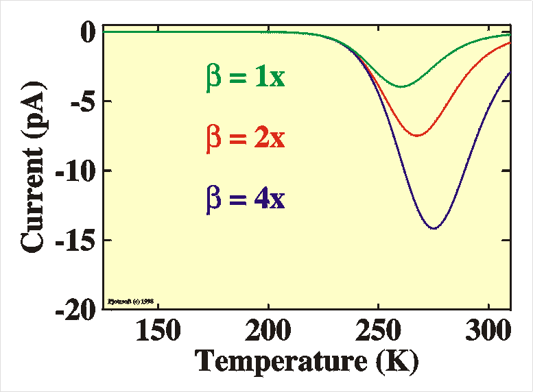 |
* We make here the assumption that all
defects in the depletion width release their charge in
a TSC experiment. More precise would be to use a value DW instead of W, where DW is the part of the depletion
width where the deep level is forced above the Fermi level with
the bias (and is below is without the bias!), see the figures a
and b in the beginning of this section.
Experimental setup
Items in an experimental set up are:
- Power supply: to be able to apply a bias voltage to the device
- (Pico)ampere meter: to be able to measure the current through
the device
- RCL (resistance-capacitance-inductance) bridge: to measure the
capacitance and the conductance (loss) of the device
- Temperature controller: to stabilize or scan the temperature
(for instance in DLTS studies)
- Optical equipment: for optical transients, or optical
spectroscopy (not discussed here)
- Computer: for steered data acquisition
The electrical schemes are shown below. For temperature dependence
measurements, the device should be mounted in a cryostat.
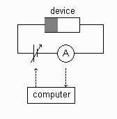
|
Setup for DC conductance (G)
measurements.
Setup for current transient
measurements.
|
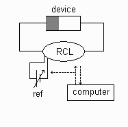 |
Setup for AC measurements
of conductance (G), loss (G/w)
and capacitance (C)
Setup for capacitance transient
measurements and DLTS
|
How does the RCL bridge work? In most cases it works like a
lock-in detector that monitors the current when an AC voltage it
applied to the device. All the current that is in phase with the
voltage is interpreted as conductance (G=1/R) and
the current that is out-of-phase is linked to the capacitance.
This is based on the properties of resistors and capacitors, IR
= V/R (Ohms law) and IC = C
dV/dt. When a sine-wave voltage Vin
is applied to the device, the currents for the capacitor and
resistor can be calculated:
Vin = Vsin(wt)
IR = GVsin(wt)
= I0
IC = wCVcos(wt) = I90
From this, the conductance can be calculated as G = I0/V
and the capacitance as C = I90/wV, with I0 the
amplitude of the in-phase current and I90 the
amplitude of the out-of-phase current. Here we made use of the
fact that sin and cos are 90 degrees out of phase. Now the trick
is how to decompose the current into the in-phase current and the
out-of-phase current parts. For this we can make use of a lock-in
detector (a.k.a. "phase-sensitive detector"). What happens is the
following:
 |
- The signal S (proportional to the current I)
is multiplied by a square wave signal with the same
period as Vin, the so-called
reference signal Vref. When the
phase of this reference is equal to the phase of the
signal S, the result is a rectification of the
signal (see the Figure).
- After rectification, the signal is put through a
low-pass filter (RC-filter). The result is a DC signal
whose amplitude is proportional to the amplitude of that
part of the input signal S that was in-phase
with the reference. If the starting signal was out of
phase with the reference, the result would have been
zero after the RC-filter, see the right part of the
Figure. The output signal is proportional to the
conductance only.
- In this way, simultaneously, two channels are used.
One channel with the reference signal in phase with
the applied voltage Vin and one
channel with the reference 90 degrees out of phase.
The first will monitor the conductance and the latter
will monitor the capacitance.
|
Measurement summary
The following table summarizes the applications of the various
measurement techniques described in this text:
|
device
structure |
shallow
level
position |
shallow
level
density |
deep
level
position |
deep
level
density |
free
carrier
mobility |
conduc-
tion
model |
interface
states |
difficulty /
cost |
| IV |
Schottky/pn
bulk |

|
|
|
|
|
|
|
1 |
| CV |
Schottky/pn |
|
|
|
|
|
|
|
3 |
admittance
spectroscopy |
Schottky/pn |
|
|
|
|
|
|
|
4 |
| IV |
FET |
|
|
|
|
|
|
|
2 |
| Hall |
bulk |
|
|
|
|
|
|
|
8 |
| TSC |
Schottky/pn |
|
|
|
|
|
|
|
3 |
| DLTS |
Schottky/pn |
|
|
|
|
|
|
|
5 |
| ToF |
bulk |
|
|
|
|
|
|
|
8 |
References
- Scientific American, July 1995.
- Physics of semiconductor devices, S.M. Sze, 2nd
edition, John Wiley & sons, 1981, ISBN 0-471-05661-8
- The Electrical Characterization of Semiconductors :
Majority Carriers and Electron States (Techniques of Physics,
Vol 14) by P. Blood, J.W. Orton, ASIN: 0125286279
- Advances in Sythetic Metals, Twenty years of Progress in
Science and Technology. ed. P. Bernier, S. Lefrant and G.
Bidan, Elsevier (1999).
- Fabrication and characterization of electronic devices
based on poly(3-methylthiophene), H.L. Gomes, PhD thesis,
University of Wales at Bangor, 1993.
- Electronic levels in MEH-PPV, ICEL-2
Conference, Sheffield. P. Stallinga, H.L. Gomes, H. Rost,
A.B. Holmes, M.G. Harrison, and R.H. Friend. Accepted for
publication in Synthetic Metals.
- Deep-level transient spectroscopy: A new method to
characterize traps in semiconductors, D.V. Lang, J. Appl.
Phys. 45, 3023 (1974).
- Charge carrier transport in poly(p-phenylenevinylene)
light-emitting device, S. Forero, P.H. Nguyen, W.
Bruetting, M. Schwoerer, Phys. Chem. Chem. Phys. 1, 1769
(1999).
- S. Karg, J. Steiger, and H. von Seggern, ICEL-2, proceedings,
Synthetic Metals (1999), and references therein.
- Microelectronic Circuits, A.S. Sedra, K.C. Smith, 4th
edition, Oxford University Press, New York (1998).
- Electronic Devices and Circuits, T.F. Bogart Jr., 4th
edition, Prentice Hall, Upper Saddle River (1997).
- Interface state mapping in terrylene, P. Stallinga,
H.L. Gomes, M. Murgia, K. Müllen, Organic Electronics 3, 43 (2002).
- Gate voltage dependent mobility of oligothiophene
field-effect transistors, G. Horowitz, R. Hajlaoui, D.
Fichou, A. El Kassmi, J. Appl. Phys. 85, 3202 (1999).
- Theory of the field-effect mobility in amorphous organic
transistors, M.C.J.M. Vissenberg, M. Matters, Phys. Rev. B
57, 12964 (1998).
- Organic field-effect transistors, G. Horowitz, Adv.
Mater. 10, 365 (1998).
- Electrical properties of single crystals of rigid rodlike
conjugated molecules, J.H. Schön, Ch. Kloc, R.A.
Laudise, and B. Batlogg, Phys. Rev. B 58, 12952 (1998).
- For the physical constants I relied on the very useful CERN
pages
http://pdg.lbl.gov/2000/contents_sports.html
It has the following official reference: C. Caso et al.,
The European Physical Journal C3 (1998) 1.
In the text the following variables and constants were used:
|
variables
|
| variable |
description |
unit |
| A |
area of the interface |
m2 |
| b |
temperature scanning speed |
K/s |
| C |
capacitance |
F |
| C0 |
background capacitance
or DC capacitance |
F |
| DC |
capacitance-transient amplitude |
F |
| cp |
hole capture rate |
1/s |
| e |
electrical permittivity |
F/m |
| ep |
hole emission rate |
1/s |
| E |
electric field |
V/m |
Epa, EA,
EA1, EA2,
Eb |
activation energies |
J |
| EF |
Fermi level |
J |
| EVB, ECB |
valence-band level and
conduction-band level |
J |
| fm |
(metal) work function |
J |
| G |
conductance (1/R) |
1/W |
| I |
current |
A |
| J, J0 |
current density |
A/m2 |
| NT, NA,
ND |
impurity densities |
1/m3 |
| Q |
total space charge |
C |
| R, Rb,
Rd |
resistance |
W |
| r |
charge density |
C/m3 |
| S |
DLTS signal |
F |
|
|
variables
|
| variable |
description |
unit |
| T |
temperature |
K |
| t, t1,
t2 |
time |
s |
| t, t0 |
life time or decay time |
s |
| Vbi |
built-in voltage |
V |
| Vbb |
total band bending |
V |
| V, VE,
VF |
applied external voltage |
V |
| Vn |
Fermi level depth in
semiconductor
relative to conduction band |
V |
| W |
depletion width |
m |
| w, w0 |
radial frequency |
rad/s |
| x |
space coordinate |
m |
| c |
electronaffinity |
V |
|
constants
|
| constant |
description |
value |
unit |
| e0 |
permittivity of vacuum |
8.854187817 ....10-12 |
F/m |
| h |
Planck constant |
6.6260755(40) 10-34 |
Js |
| k |
Boltzmann constant |
1.380658(12) 10-23 |
J/K |
| q |
elementary charge |
1.60217733(49) 10-19 |
C |
Note: the units presented here are
according to S.I.
In reality often different units are
encountered. For
instance, energies are nearly always
given in eV
(1.6 10-19
J) , depletion widths in nm or Å
and impurity levels in cm-3
|
 page written and
maintained by Peter Stallinga,
page written and
maintained by Peter Stallinga,
Source written in HTML with NetScape 4.76. Pictures
made with PjotrSoft (my software name), output in PostScript
format. Converted with Corel Draw, GhostView, LViewPro and GIMP
(Linux) into GIFs.
In no way were any electrons harmed in the process!
Copyright © 1999-2007, Universidade do Algarve