 |
Theory of Metal-Insulator-Semiconductor Field-Effect Transistors (MOS-FET) |
|
Theory of Metal-Insulator-Semiconductor Field-Effect Transistors (MOS-FET) |
 When I
wrote this in
2004, I tried to make theory pages for our research on organic
thin-film transistors (TFTs). At that time, I did, just
like everybody else, make the assumption that a thin-film
transistor is
just like a thin MOS-FET. Any theory of a MOS-FET I assumed to be
directly applicable to a TFT. This, however, proved to be wrong.
Recently we developed a theory specially designed for thin-film
transistors
(organic and inorganic alike). Click here
(http://www.ualg.pt/fct/adeec/optoel/theory/tft/) if you
want to study TFT
instead of MOS-FETs. These pages now exclusively deal
with MOS-FETs. At this moment, these pages are no longer relevant
to our research, but I keep them because they might anyway be
interesting for some people.
When I
wrote this in
2004, I tried to make theory pages for our research on organic
thin-film transistors (TFTs). At that time, I did, just
like everybody else, make the assumption that a thin-film
transistor is
just like a thin MOS-FET. Any theory of a MOS-FET I assumed to be
directly applicable to a TFT. This, however, proved to be wrong.
Recently we developed a theory specially designed for thin-film
transistors
(organic and inorganic alike). Click here
(http://www.ualg.pt/fct/adeec/optoel/theory/tft/) if you
want to study TFT
instead of MOS-FETs. These pages now exclusively deal
with MOS-FETs. At this moment, these pages are no longer relevant
to our research, but I keep them because they might anyway be
interesting for some people.As we will see, the MIS-FET can be well described by a MIS-diode with source and drain electrodes connected in the plain of the active layer. Therefore, it is best to start with the MIS junction.
::: MIS junction.
::: Capacitance of an MIS junction
::: Field-Effect transistor (inversion channel)
--
Linear region
--
Threshold voltage of an inversion-channel FET
--
Subthreshold region of an
inversion-channel
FET
--
Saturation
--
Short-channel effects
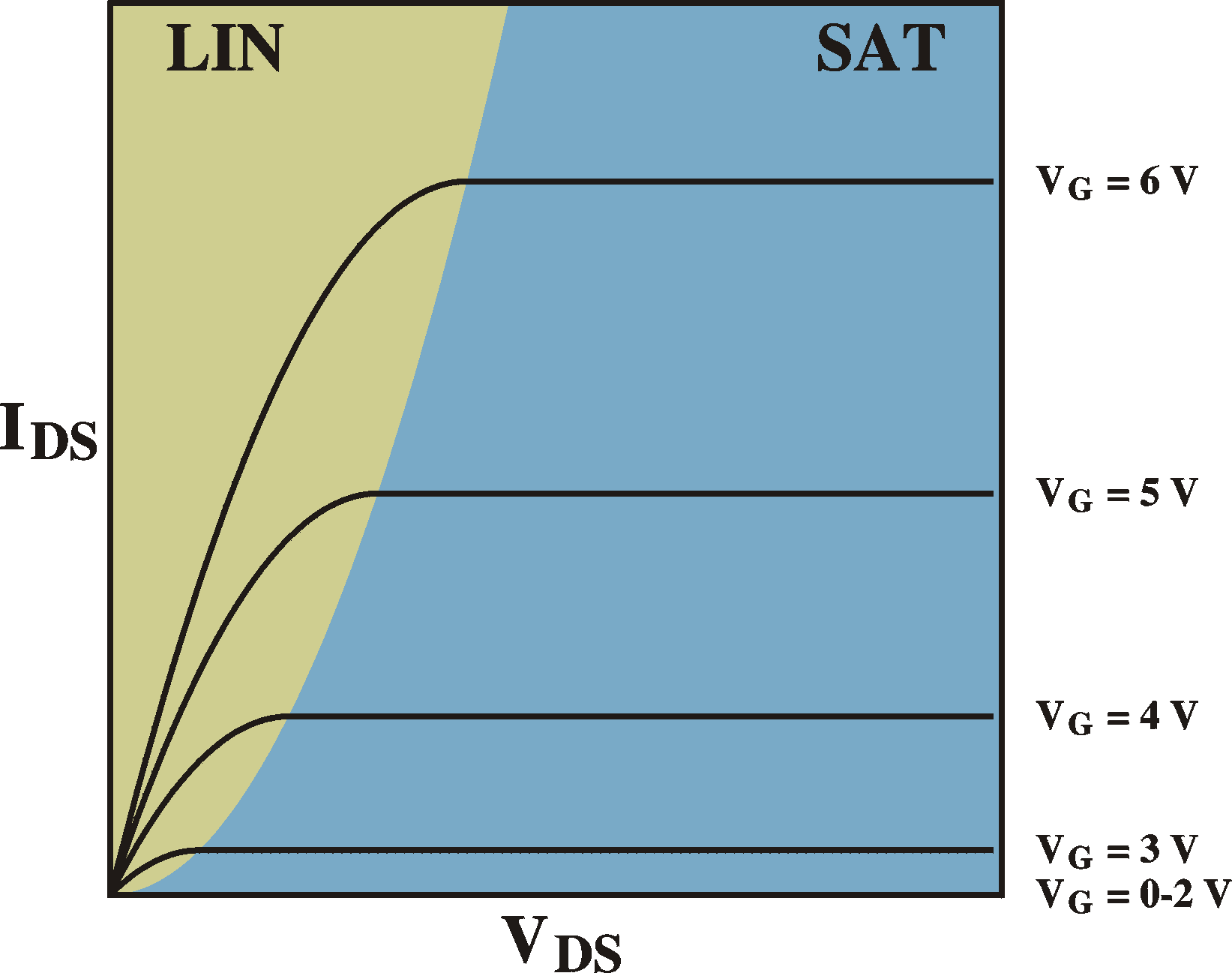
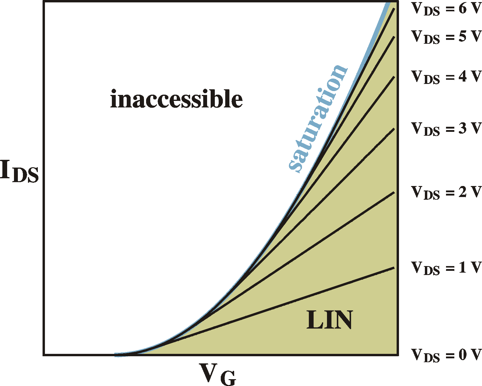
To understand how an FET (of the MOSFET type) works, we first have
to analyze what an MIS structure is.
In a simple approximation, a MOSFET is a planar device of
semiconducting
material whose free carrier concentration n, and hence it
conductivity
(via g = men)
is
controlled
by the gate.
The first figure shows an energy diagram of an MIS device. The
device
consists of a metal and a semiconductor separated by an insulator.
Here
we assume that the insulator is not conducting any current.
Standard textbooks start with an ideal MIS device, which means
that
the Fermi levels in the metal and the semiconductor are aligned
even
before
contact. In other words, the work functions of the metal and of
the
semiconductor
are equal, fm = c
+ EC-EF.
This
implies
that we have no band bending in the absence of external voltages.
Remember
the Schottky barrier, where charge was flowing from one side to
the
other
due to the misalignment of the Fermi levels. In the ideal MIS
junction
such a flow of charge is not needed (which saves us the trouble of
explaining
how it can pass through the oxide :-)
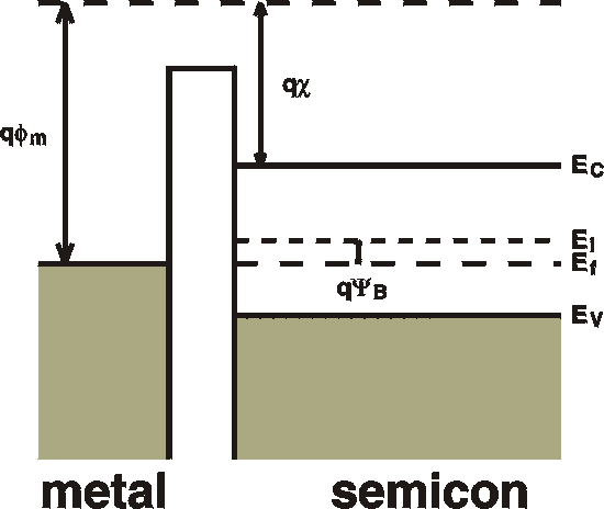 |
fm : the
metal
workfunction.
How much it costs to take an electron from the top of the
sea of
electrons
in the metal to vacuum. The "workfunction" of the
semiconductor can be
defined as c + EC-EF. fb : (not shown, because it doesn't enter into the calculations): the barrier height of the oxide as seen from the metal; the difference between the "conduction band" of the oxide and the Fermi level of the metal.. c : the electron affinity of the semiconductor. The energy it takes to take an electron from the conduction band to the vacuum level. EG : energy gap of the semiconductor. YB : the energy from the midgap level to the Fermi level. This is approximately equal to EG /2 EC : bottom of conduction band. EV : top of valence band. |
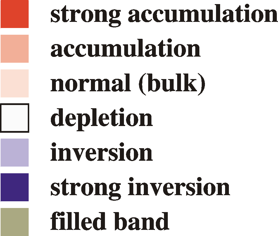
| The following strip explains what happens when we
connect an
external
voltage to the metal (gate). For that we use the legend as
shown here
on the right.
Note that the (horizontal) SCALE of the pictures is changing. Just like in Schottky barriers, the depletion width depends on the voltage. Here the depletion width is shown as constant. |
 |
| a) Depletion 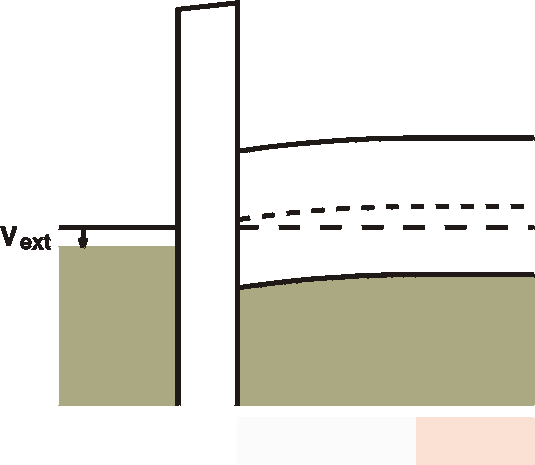 |
When a small (positive) voltage is connected to the metal (gate), free holes are pushed out of the interface region and a band bending results on the other side of the insulator. This is the same effect as seen in a Schottky barrier. Free carriers (holes) flow out of the interface region and a depletion zone is formed. The uncompensated (negatively) ionized acceptors cause an electric field and - via Poisson's equation - a parabolic bending of the bands. Note that there is also a voltage drop in the oxide. In the oxide no charges can reside and hence the field is constant and the voltage drop is linear in space. The total voltage drop in the oxide plus the band bending is equal to the external voltage. |
| b) Inversion 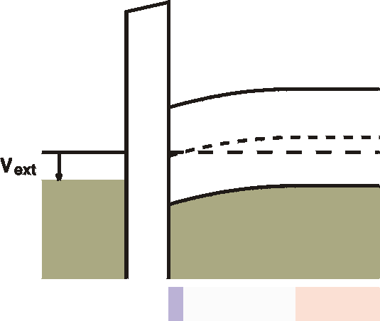 |
When the voltage is further increased, at the interface an inversion region is created. The semiconductor becomes here n-type, albeit not very conductive, yet. |
| c) Strong Inversion 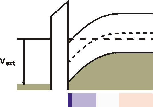 |
For very strong bias, the Fermi level crosses the conduction band close to the interface. This is strong inversion. Free electrons are in a so-called "channel" next to the oxide. This channel is therefore highly conductive. The ample availability of states in the conduction band means that further increases in the gate voltage will not extend this strong inversion region into space, but rather will increase the density of electrons in the channels. The channel is always infinitesimally thin.The huge amounts of free carriers can easily cause a large voltage drop (band bending) and only a thin layer is needed to "absorb" the external voltage. Note that the depletion width (the white zone) and the inversion width (light blue zone) are constant once the channel is formed. |
| d) Accumulation 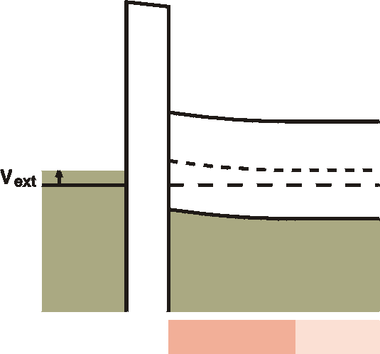 |
Going in the other direction, a negative voltage at the gate metal will attract some free holes to the interface. In this accumulation region, an increased number of free holes is created, although it is not yet dramatic; the interface is still high-ohmic. |
| e) Strong accumulation 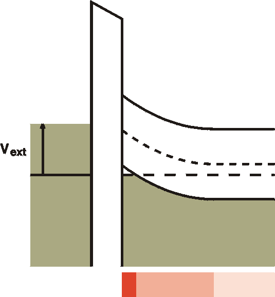 |
For stronger negative voltages at the gate the Fermi level is forced below the valence band at the interface. A channel with high density free holes is created. This is called strong accummulation. Again, as for the strong inversion case, further increasing the voltage will result in an increase of the density of the free holes rather than an increase of the channel in space. In the picture the width of the channel is exaggerated. In reality it is only a monolayer thick. |
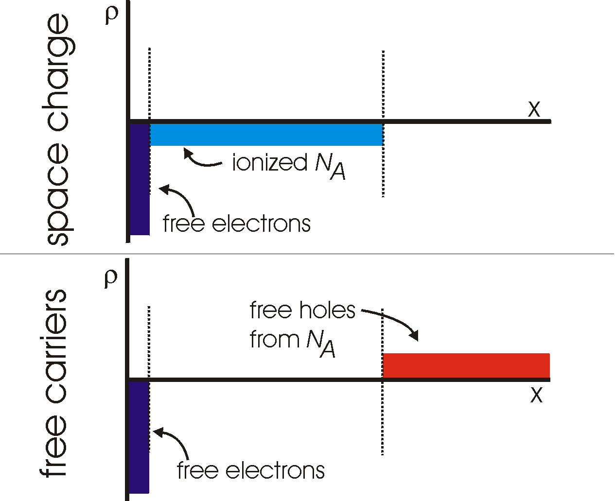
To complete the story, in strong inversion we have the following distribution of space charge and free carriers:
|
|
||
| depletion: Cd = | ----------- | accumulation: Ca = Cox |
| Cox + CW |
 or Fig. 4-3-5a on p. 348 of Shur .
For high frequencies, the depletion zone is not short circuited and
the
measured capacitance is a series capacitance of the oxide and the
depletion
width. The depletion width is constant once it is fully formed (see
images
above) and we will measure a constant capacitance.
or Fig. 4-3-5a on p. 348 of Shur .
For high frequencies, the depletion zone is not short circuited and
the
measured capacitance is a series capacitance of the oxide and the
depletion
width. The depletion width is constant once it is fully formed (see
images
above) and we will measure a constant capacitance.
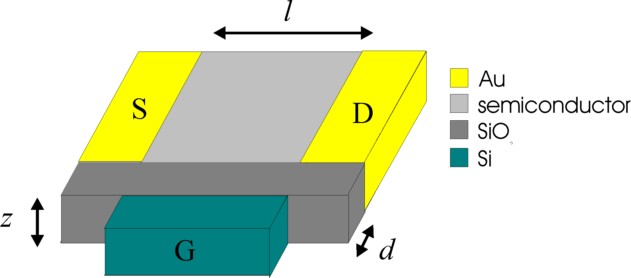 |
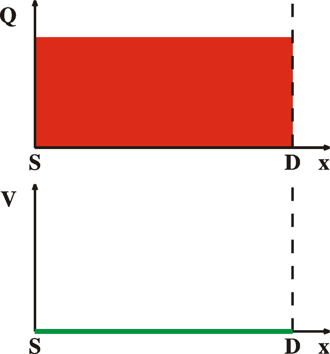
Directions: x: from oxide to surface of film y: from source to drain z: along an electrode Z: electrode width |
Under the assumption that all the free carriers come from charges
in
the strong accumulation or depletion zone, it is very easy to
calculate
the amount of charge on the semiconductor side and hence the
current.
In
the section above we have seen that the capacitance of an MIS
junction
under these conditions is equal to the oxide capcitance, Cox.
Assuming no other capacitances, all the charges go to the
interface and
therefore, since C = Q/V we find Q
=
Cox VG. As written
above,
we need VT to bring it into strong accumulation
or
depletion,
therefore Q = Cox
(VG
-VT).
With this in mind, and with the idea that the conduction is
proportional
to the charge as seen in equation I the current in the linear
region
becomes
|
IDS = Cox (VG -VT) mVDS Z/L |
 |
 |
Remember that we arrived at this by the assumption that all the
free
carriers are located in the strong inversion or accumulation zone
close
to the interface and that the rest of the device is not
conducting.
Especially
in materials with bulk Fermi levels close to the band edges, the
background
conductivity (the "off current") can be very large. In principle,
the
purer
the material, the closer the Fermi level will be to mid gap and
the
less
off-current we will have. Making the films thinner also helps.
Moreover, not all the charge induced by the gate is free charge.
The
above model is also known as the Charge Control Model. If we do
include
the background conduction in the bulk and the depletion and
inversion
zones,
we have to add a term to the above equation, to arrive at the
Schottky
model, see Sze
and Shur .
|
VT = (4qesyBNA)1/2 / Cox + 2yB |
As an example: for NA = 1x1016 cm-3,
Cox
= 50 mF/m2,
EG
= 2.5 eV (yB = 1.25 V), es
= 5.0e0 we get VT
= 11.9 V + 2.5 V = 14.4 V; since the first term in the equation
comes
from
the oxide and the second term comes from the semiconductor we can
see
that
most of the external voltage (83%) is absorbed by the oxide
(remarkably).
The Fermi level, of course, also depends on the acceptor
concentration,
so in total we get a complex dependence on NA.
In
textbooks,
it is assumed that all acceptors are ionized. In fact, for organic
materials,
where the acceptor level can be very deep (but abundant) this is
not
necessarily
the case. In fact, we should read NA as
"ionized
levels"
and this can be a fraction of the real number of acceptors, unlike
in
classical
materials such as Si and GaAs. Moreover, the fraction of levels
ionized
can be changed by changing the band bending (by applying a gate
voltage)
and thus, the threshold voltage can change when putting the device
in
operation.
Depending on the depth of the levels, these changes can be in the
order
of seconds, to minutes and hours and even days.
Note that high levels of current have no effect on this trapping
of
charges, since they do not attribute to a different band bending
or
extra
charges in the interface.
Note that for an accumulation type FET this calculation does not
work
because we do not have a space-charge region caused by ionized
acceptor
levels; VT does then not depend on NA.,
but
only on the Fermi level and the number of valence band states.
Remark: We have considered here an FET without a wire connected to the bulk of the device. If we do so, the threshold voltage reduces to VT = (2qes(yB-Vsub)NA)1/2 / Cox + 2yB, with Vsub the voltage of the substrate.
If you do the calculation correct, you will see that the distance
of
the Fermi level depends linearly on the gate voltage and with a
square-root
on the acceptor density NA. Hence the current
follows
something like (Sze ,
Szur )
 NA]
NA]
If we assume a linear voltage drop from source to drain from 0 to 10 V, we can exactly calculate where the channel closes, namely at 10% distance from the drain. We have to bear in mind, though, that a closed channel has less free carriers and thus has higher resistivity. The law of continuity tells us that the current at every place of the device must be equal. Therefore, since voltage drop is current times resistivity, the voltage drops much faster in a closed-channel region than in a open-channel region. Moreover, if we assume that the free-carrier density in the closed-channel region is much smaller than the open-channel region, the pinch-off region is very small.
The voltage of start of saturation is easy to calculate. At this voltage the gate-drain voltage is exactly equal to the threshold voltage. VG-VD = VT. Thus (VS = 0, VD = VDS)
onset of saturation: VDS = VG-VT
Beyond this voltage, the current is constant. We will have a region from the source to near the drain with a voltage drop of VG-VTand a very thin region close to the drain with the rest of the voltage drop of VDS. The length of the first region is nearly independent of the total external voltage. It therefore has a contant length and voltage drop, and the current through it is therefore independent of VDS. Again, continuity tells us that the current at every point is equal, therefore, the saturation current is independnet of VDS.
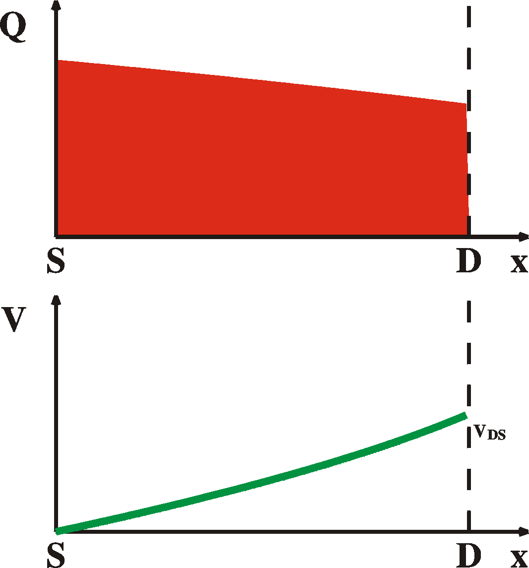
With this we can calculate the free carrier density Q(x)
and the voltage V(x) of every point in the channel
at
the
onset of saturation. Along the way we will also calculate the
current
which
is the current in saturation.
Imagine putting up a screen at a distance x from the
source,
peprpendicular to the source-drain direction, stretching as long
as the
electrode lengths (Z) and as high as the film thickness. We can
calculate
the current I through such a screen.
The current I at a crossection at a certain point x
is
equal to the free-charge density at that point Q(x),
the
carrier mobility m and the local field
E(x)
= dV(x)/dx:
I(x) = ZmQ(x)
dV(x)/dx
Because of continuity, this current has to be constant along x
and equal to the drain-source current IDS. The
above
equation then reduces to
dV(x) / dx = IDS/ZmQ(x)
(eq.I)
The free-carrier density is a function of the local field VG-V(x),
as seen before:
Q(x) = Cox[VG-V(x)-VT]
(eq.II)
The solution to this system of diferential equations is easy (take
the derivative of the second equation and put this in the first),
to
which
we add the following boundary condition:
1a: the charge at the drain is zero: Q(L)
= 0.
1b: The voltage at the drain is just enough to
close
the channel: V(L) = VG-VT.
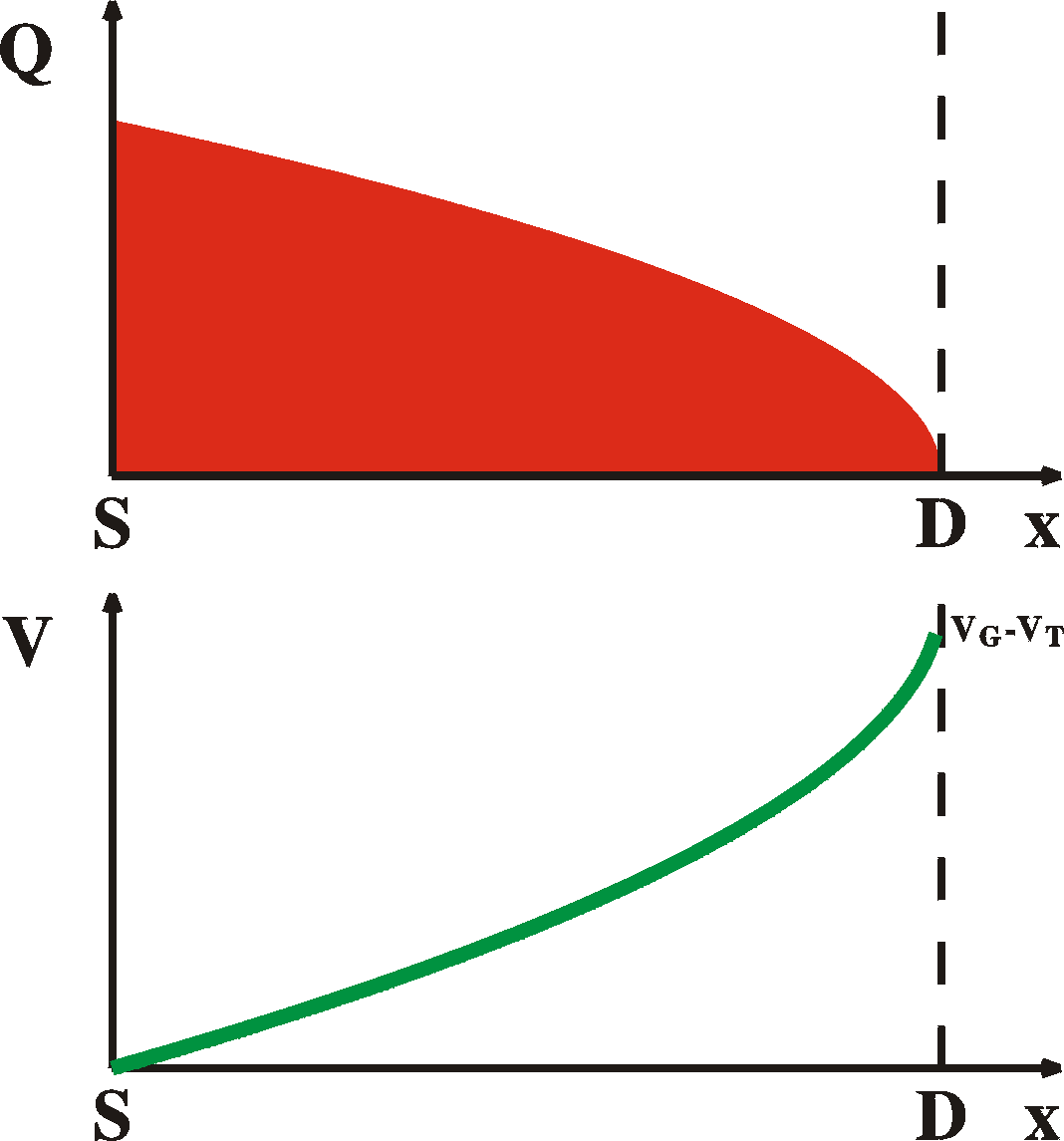 The
soulution is then The
soulution is then Q(x) = [(2CoxIDS/Zm)(L-x)]1/2 V(x) = (VG-VT) - [(2IDS/mZCox)(L-x)]1/2 Using the next boundary condition 2a: The voltage at the source is 0: V(0) = 0 2b: The charge at the source is Q(0) = Cox (VG-VT) we can calculate the current |
|
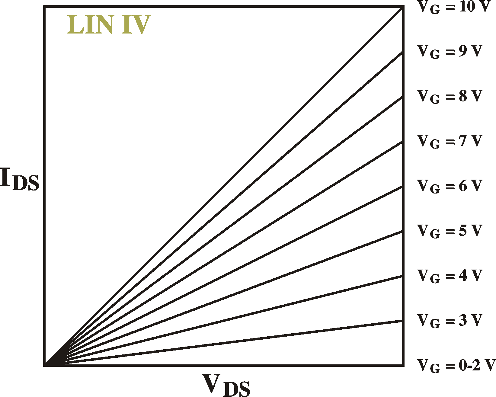
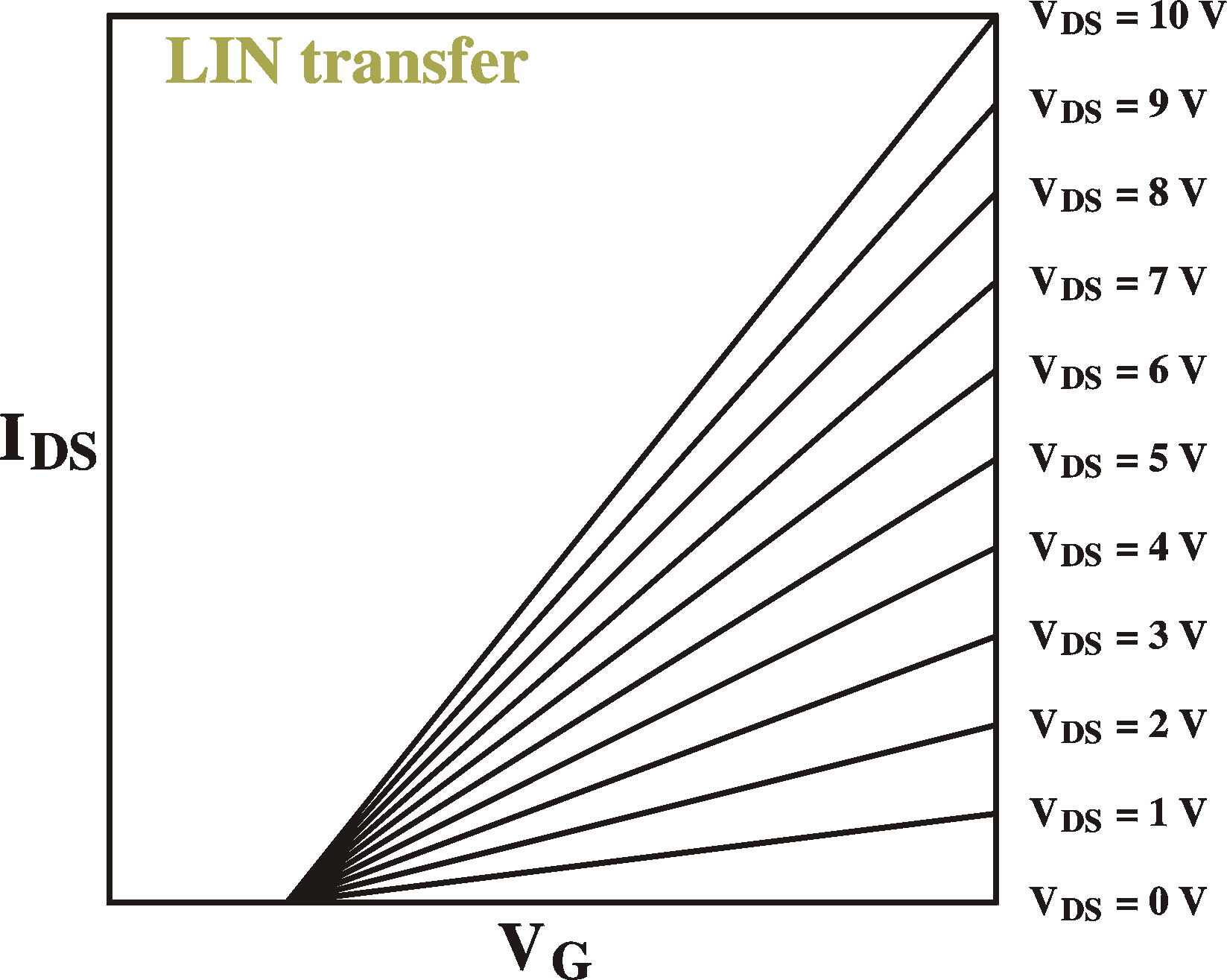
IDS = (1/2)m(Z/L) Cox (VG-VT)2 |
which is the current at the onset of saturation and,
since,
as
we have shown before, the current beyond this point is independent
of VDS,
this is the current in saturation (as long as VG
< VDS + VT).
The total amount of charge stored in the device in saturation can
be
found by integrating the equation for the charge distribution
above and
multiplying by the device width Z:
at saturation, VDS = VG-VT:
Q = (2/3) Z (VG-VT)
Cox
in the same way:
at VDS = 0 V
:
Q = Z (VG-VT)
Cox
Note: when we increase the bias, charge is coming out of the
device.
We have to be careful in our IV measurements that we do not
measure the
current of these charges going into and coning out of the device.
See
the
section on displacement current.
We can also use the same method to calculate the current before
saturation.
Going back to the general solution of the system of differential
equations:
V(x) = (VG-VT)
-
[(2IDS/mZCox)(x0-x)]1/2
As boundary conditions we now take:
1: The voltage at the source is 0; the charge
is
Cox
(VG-VT)
2: The voltage at the drain is V(L)
= VDS
The result is
|
IDS = m(Z/L) Cox [(VG-VT)VDS - (1/2)VDS2] |
 |
 |
For completeness sake and for later reference, here are the
charge
distributions
and voltage curves for the different regimes, ranging from 1)
equilibrium,
2) linear regime, 3) onset of saturation, 4) in saturation.
 |
 |
|
 |
|
|
LIN |
onset of SAT |
SAT |
|
Note: the units presented here are
according
to S.I. |
||||||||||||||||||||||||||||||||||||||||||||||||||||||||||||||||||||||||||||||||||||||||||||||||||||||||||||||||||||||||||||||||||||