
Theory of electrical characterization
of (organic) semiconductors
by Peter Stallinga
Universidade do Algarve
 |
Theory of electrical characterization of (organic) semiconductors by Peter Stallinga Universidade do Algarve |
| Then the next question is: why are some organic materials
(polymers)
semiconductors? The answer is well described in section IVB
of Chapter
2 of "Advances in Synthetic Metals, Twenty years of Progress
in Science
and Technology" |
|
With a bandage of 2.5 eV the polymer would not be conducting at all. This distance between the valence band and conduction band is much too large to allow for free carriers to be generated at room temperature. For that too happen, an electron would have to acquire huge thermal energy to make the jump to the conduction band. There are still some ways that we can have free carriers in the polymer:
For the theory presented here it doesn't matter what shape the
carriers
take. We will assume that all carriers are free carriers.
One
important
difference between classical semiconductors and polymers is worth
to be
pointed out here, though. In classical materials, the conduction
is
always
3-dimensional, while polymers are 1-dimensional conductors. Or, at
least
there is an anisotropy; the conduction in one dimension is better
than
in the other two. Hence, there exist (at least) two processes for
conduction
with two activation energies. One for conduction along the chain
and
one
for "hopping" to near chains.
|
|
|
|
| ohmic contact | IV curves Hall measurement |
transport model, shallow level mobility |
| Schottky barriers
p-n junctions |
IV CV DLTS TSC admittance spectroscopy |
transport model, barrier height shallow level, barrier height deep states deep states shallow level, deep levels, dielectric constant e |
| FETs | IV | mobility |
| acoustic phonons: | mp ~ m*-5/2T-3/2 |
| ionized impurities: | mp ~ m*-1/2T3/2 |
| optical phonons: | mp ~ m*-3/2T1/2 |
In principle we can determine the activation energy for bulk
conduction
through the measurement of the conductivity as a function of
temperature.
Normally the resistivity is measured with a four-point
probe. Two
points are applying a current and two other points are measuring
the
voltage.
The resistivity of the sample in the simple model does not depend
on
the voltage. In more sophisticated models it does, but they
will
not be described here.
If we know the parameters of the device we can find the mobility directly from the DC measurements. Otherwise, we have to resort to FETs, Hall measurements, or Time-of-flight measurements, see the chapter on measuring mobility.
For insulating materials, the transport can be of yet another type. In general, it has a stronger field-dependence. Examples:
Fowler-Nordheim tunneling
Poole-Frenkel
 |
 |
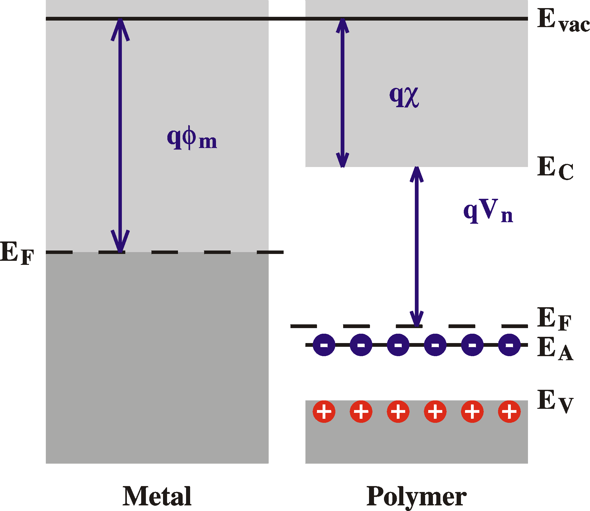
| A metal and a semiconductor before contact. Note
the different Fermi levels which will cause electrons to flow to the semiconductor. |
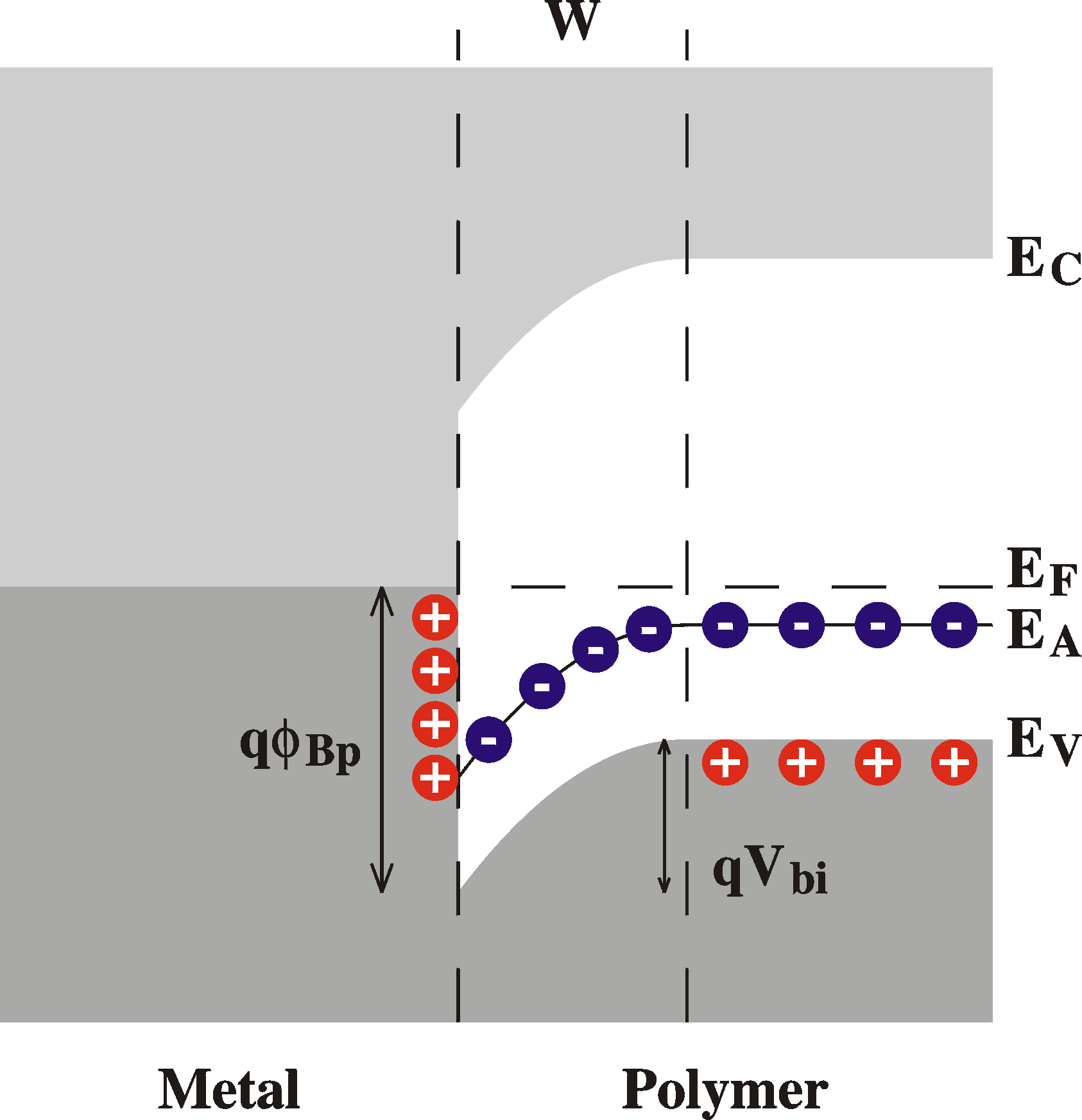
A Schottky barrier formed after contact of the metal and the semiconductor. A region of un- compensated charged acceptors results. This "space charge" causes a voltage drop at the interface. |
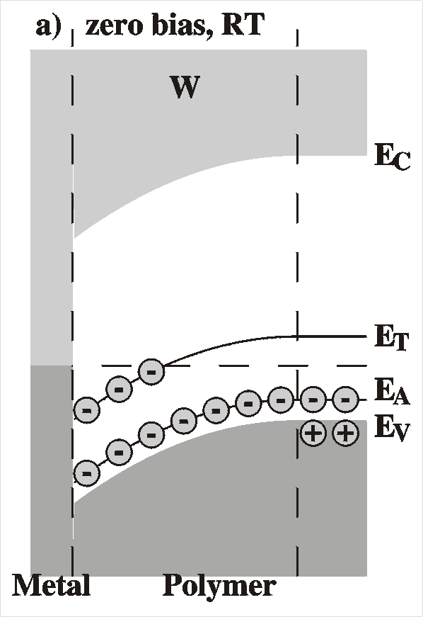
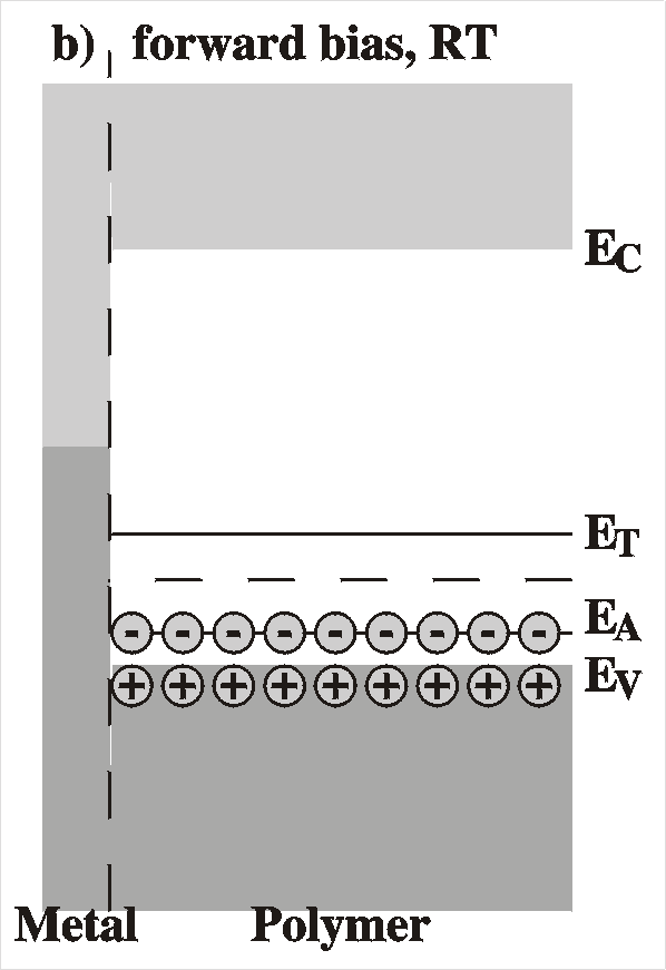
At equilibrium, in the absence of externally applied voltages, the Fermi level must be constant throughout the sample, since otherwise a current would flow. In the metal the Fermi level is the top of the electron sea, while in the semiconductor, far from the interface, the Fermi level is determined ("pinned") by the impurity level. The Fermi level is matched in the following way: Before equilibrium, the Fermi level is lower in the semiconductor (when the work function of the polymer, Evac-EF = c + Vn, is larger than that of the metal, fm), therefore, electrons will flow from the metal to the polymer. This causes the build up of charges on both sides of the interface, resulting in an electric field and therefore a potential gradient according to Poisson's equation d2V/dx2 = r(x). This is the so-called band bending. In this region, the electric field has caused the holes to move away from the interface; they drift to the top of the valence band. The result is that in this area -- of width W -- there is a surplus of negative charge caused by uncompensated charged acceptors, the "space charge region" or "depletion region", since there is an absence of majority carriers (holes in p-type semiconductors).
The parameters that describe the Schottky barrier are:
Similar to the Schottky barrier we have a pn-junction (of two
equal
semiconductors with different doping details) or a hetero-junction
(of
two different semiconductors). The theory of these devices
is
rather
similar and will not be mentioned here further.
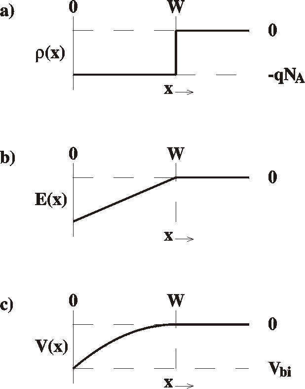 The
depletion width of a Schottky barrier can be calculated from
Poisson's
equation
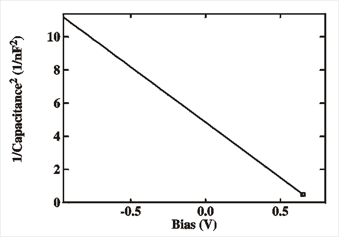 This
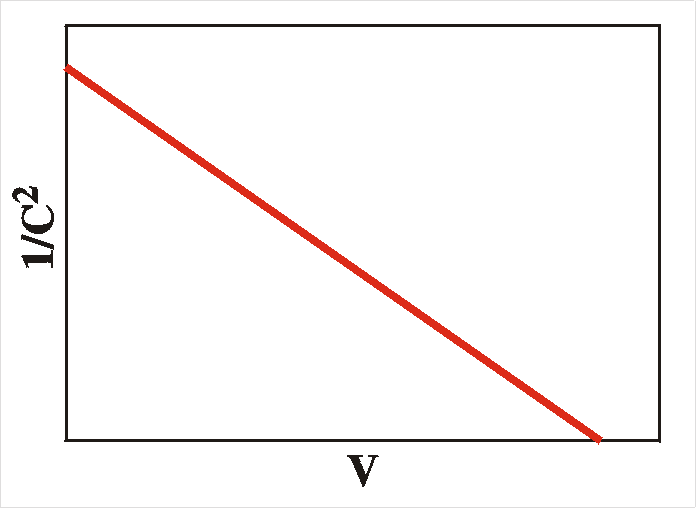
shows that a Mott-Schottky plot (C -2
vs. V) is a straight line and the slope reveals the acceptor
concentration.
The Figure shows an example of a system with an acceptor concentration of 4.28 1015 cm-3 and a built-in voltage of 0.75 V.
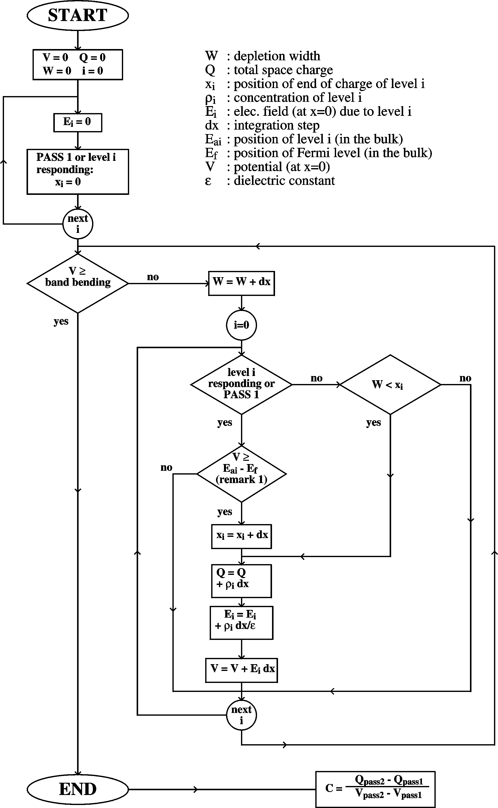 |
The Figure above shows an algorithm used for calculating
depletion
widths
and capacitances for Schottky barriers ("view image" to see it in
more
detail). As an example, consider the situation of a system
with
two
homogeneously distributed acceptor
levels, one 0.1 eV and the other 1.0 eV above the valence band
with
the Fermi level at EVB + 0.6 eV. Both have a
concentration
of 1016 cm-3. For
e=5,
a dot diameter of 2 mm, and a built-in voltage of 0.8 V, the
Mott-Schottky
plot is given in the Figure.
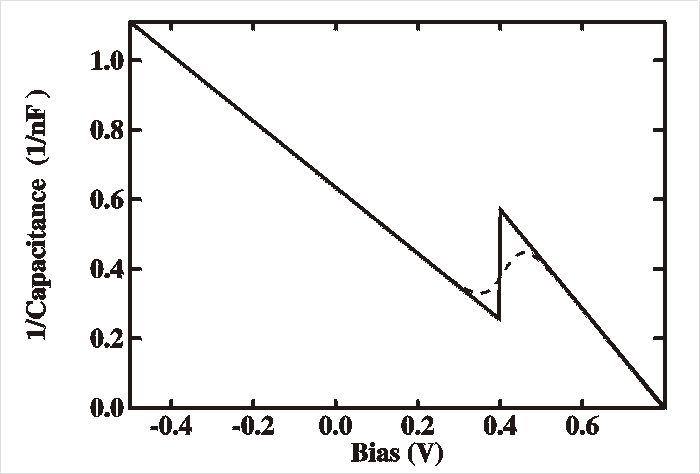 The
Figure shows a simulation of a C-2V
plot
of
a two-level system as described in the text. For voltages
higher
than 0.4 V (built-in voltage - ET1-EF
the band bending is not large enough to put the deepest level
below the
Fermi level anywhere. Hence the space charge is only a result of
the
shallow
level and we see a large slope (small concentration). For lower
voltages,
or reverse voltages, both levels contribute to the space charge
and
both
are visible in the slope which is now much smaller. Note that the
sharpness
of the transition is due to the assumption that around the Fermi
level
the levels are either completely full or completely empty
(emulating 0
K). The situation for T=300 K is shown with a dashed line.
Note
also that the two slopes do not point to the same built-in voltage
Vbi.
The
slopes
will still yield the correct acceptor concentrations,
though.
The
Figure shows a simulation of a C-2V
plot
of
a two-level system as described in the text. For voltages
higher
than 0.4 V (built-in voltage - ET1-EF
the band bending is not large enough to put the deepest level
below the
Fermi level anywhere. Hence the space charge is only a result of
the
shallow
level and we see a large slope (small concentration). For lower
voltages,
or reverse voltages, both levels contribute to the space charge
and
both
are visible in the slope which is now much smaller. Note that the
sharpness
of the transition is due to the assumption that around the Fermi
level
the levels are either completely full or completely empty
(emulating 0
K). The situation for T=300 K is shown with a dashed line.
Note
also that the two slopes do not point to the same built-in voltage
Vbi.
The
slopes
will still yield the correct acceptor concentrations,
though.
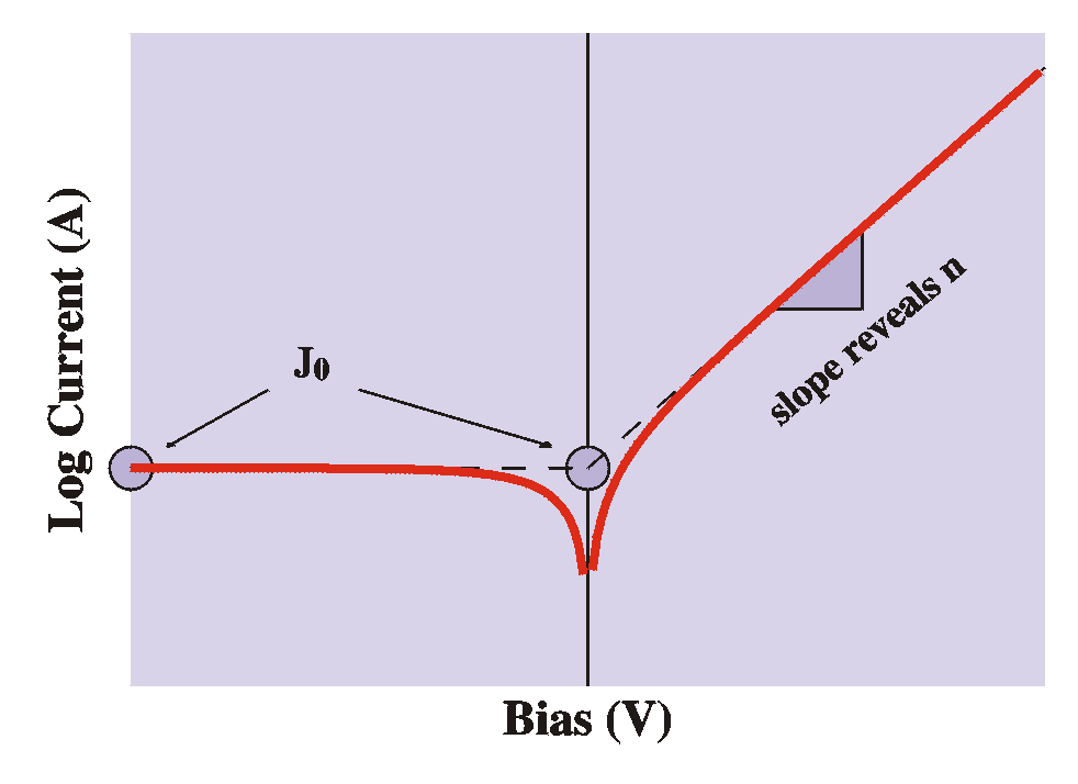
Alternatively, the current can be following the diffusion theory:
Finally, a combination of the two theories, the thermionic emission-diffusion theory predicts a current following the equation
The currents are all of the form
|
|
|
 |
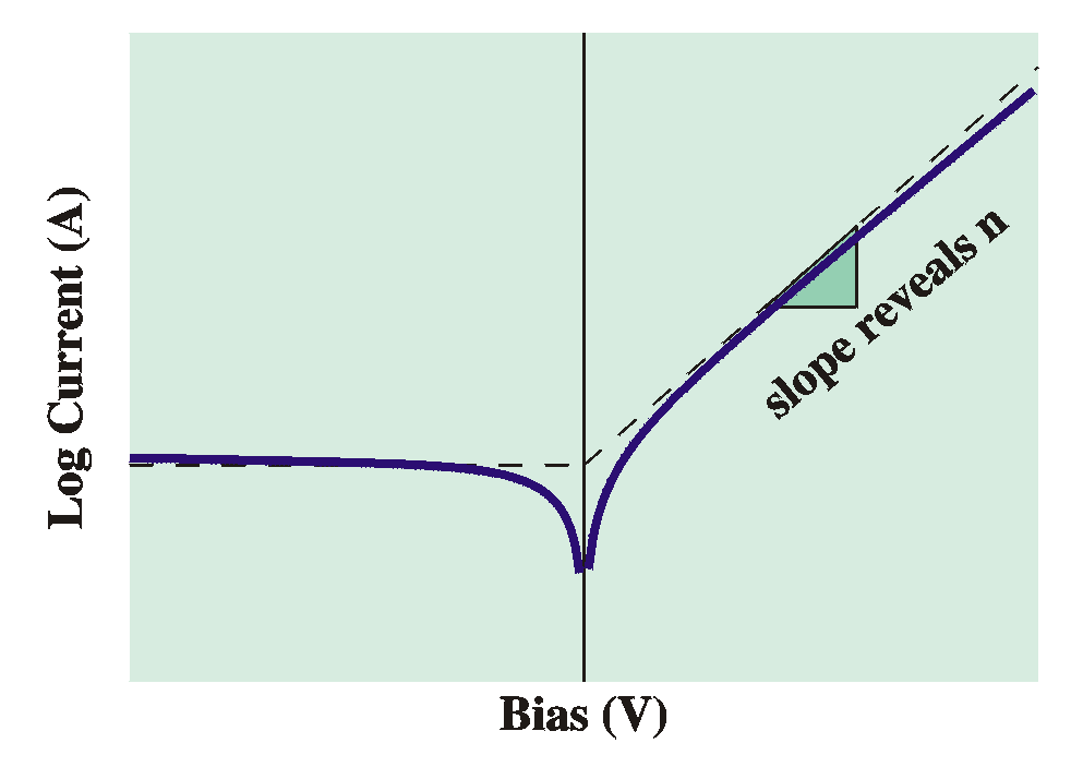 |
From a DC current-voltage plot ("IV plot") we can determine
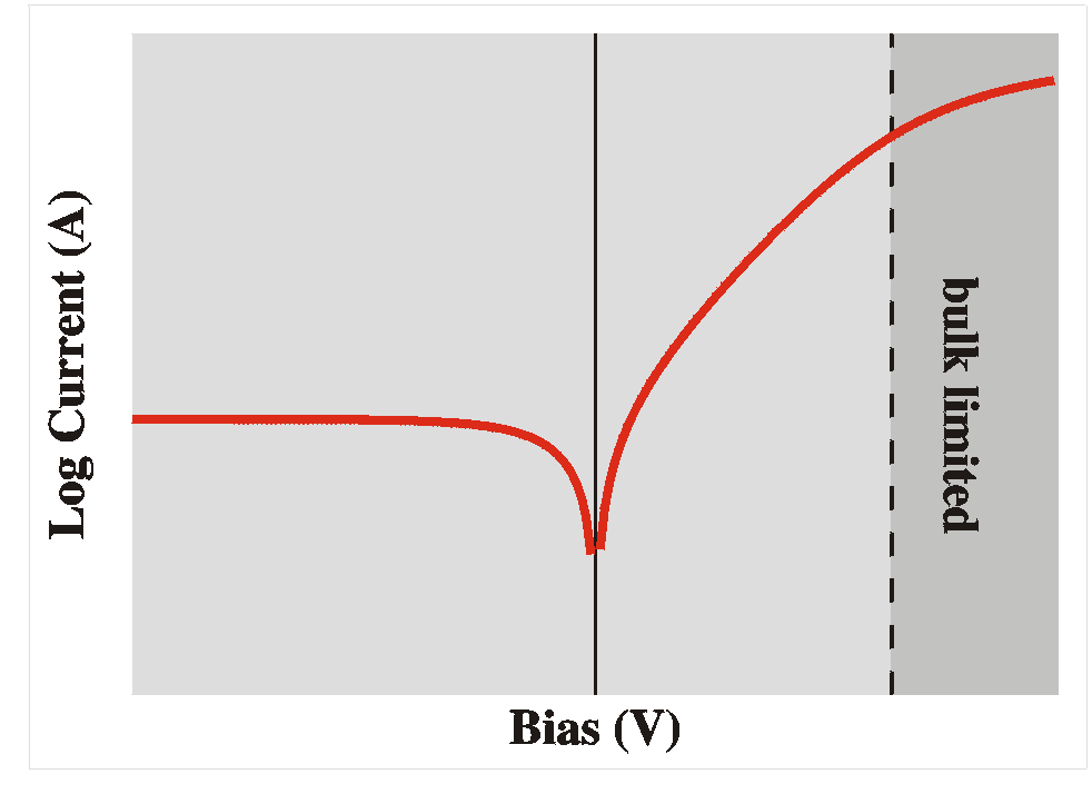 |
A final note: For high forward voltages, the current may
be
limited
by the resistivity of the bulk. In that case, the current
doesn't
continue
to rise exponentially with the bias, but only grows
linearly. In the
semi-log
IV curves this is visible as a bending of the curve at
strong forward
bias. Since the current is limited by the bulk conductivity we can again apply the theory for bulk samples. |
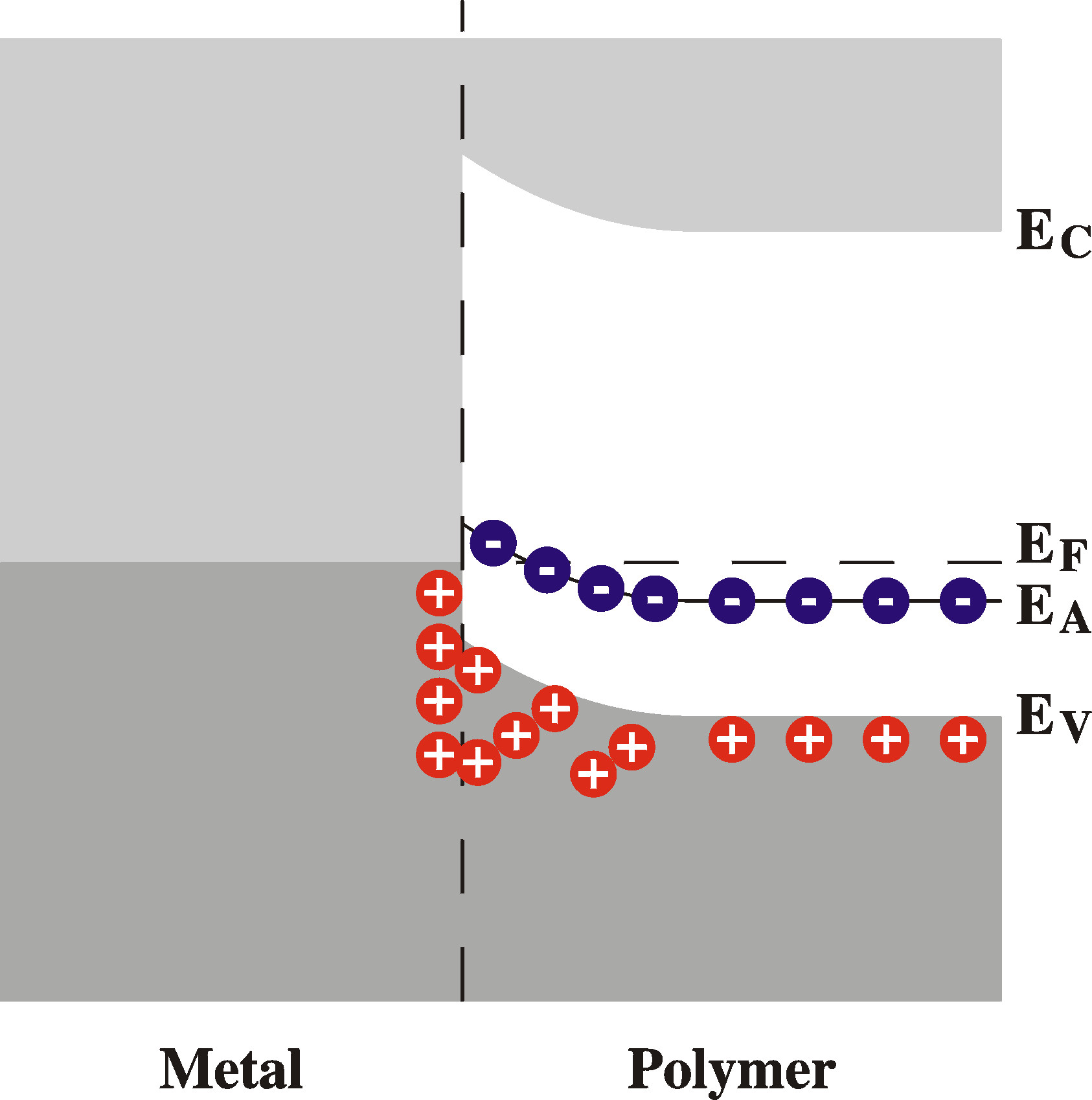 A
special case is when the currents are limited by the space
charge. This
means that the density of free carriers injected into the
active region
is larger than the number of acceptor levels. It is easy to
see that we
then go from situation of band bending caused by
uncompensated ionized
acceptor levels to the case of band bending caused by over-compensated
acceptor levels. The band bending is then in the other
direction (!).
The
local field the carriers feel when injected into the active
region is
then
driving them out of there and back into the contact
electrode. The
entire
current must come from the diffusion of carriers. In other
words, the
current
is caused by the large gradient of density of free carriers. A
special case is when the currents are limited by the space
charge. This
means that the density of free carriers injected into the
active region
is larger than the number of acceptor levels. It is easy to
see that we
then go from situation of band bending caused by
uncompensated ionized
acceptor levels to the case of band bending caused by over-compensated
acceptor levels. The band bending is then in the other
direction (!).
The
local field the carriers feel when injected into the active
region is
then
driving them out of there and back into the contact
electrode. The
entire
current must come from the diffusion of carriers. In other
words, the
current
is caused by the large gradient of density of free carriers.
Instead of the simple approximation with only the drift current I = qmenE we have the more comples form including both the drift current and the diffusion current: I = qmenE + qDn dn/dx In fact, the drift current is opposing the diffusion current as can be seen in the figure; the electric field will drive the holes back to the metal. In general, we can expect space charge limited currents (SCLC) when the acceptor density is small (and the band-bending and E becomes negative for large amounts of injected carriers) or when the mobility of the carriers is small (so that the first term in the equation above becomes negligible compared to the second term), especially when and where the charge-density gradient dn/dx is large. |
The Bell Labs group of Schön and Batlogg gives a nice
summary
of
these measurements ![]() (PRB
58), which, in turn, is based on chapter 7.3.4. of
Sze
(PRB
58), which, in turn, is based on chapter 7.3.4. of
Sze ![]() .
The DC current of a device can be devided into the following
types:
.
The DC current of a device can be devided into the following
types:
In the Ohmic regime, the current is proportional to the
electric
field. This is equal to a simple resistance.
The space-charge-limited-current regime (SCLC) occurs when
the
equilibrium charge concentration (before charge injection) is
negligible
compared to the injected charge concentration. This will form a
space
charge
cloud neaar the injecting electrode; the concetration of the space
charge
rapidly dies out away from the electrode. In this regime, the
current
is
proportional to the square of the electric field.
With the bias, the trap levels are filled. Above the trap-free
voltage
limit, the traps are filled and the device enters the trap-free
SCLC.
The figure below summarizes this.
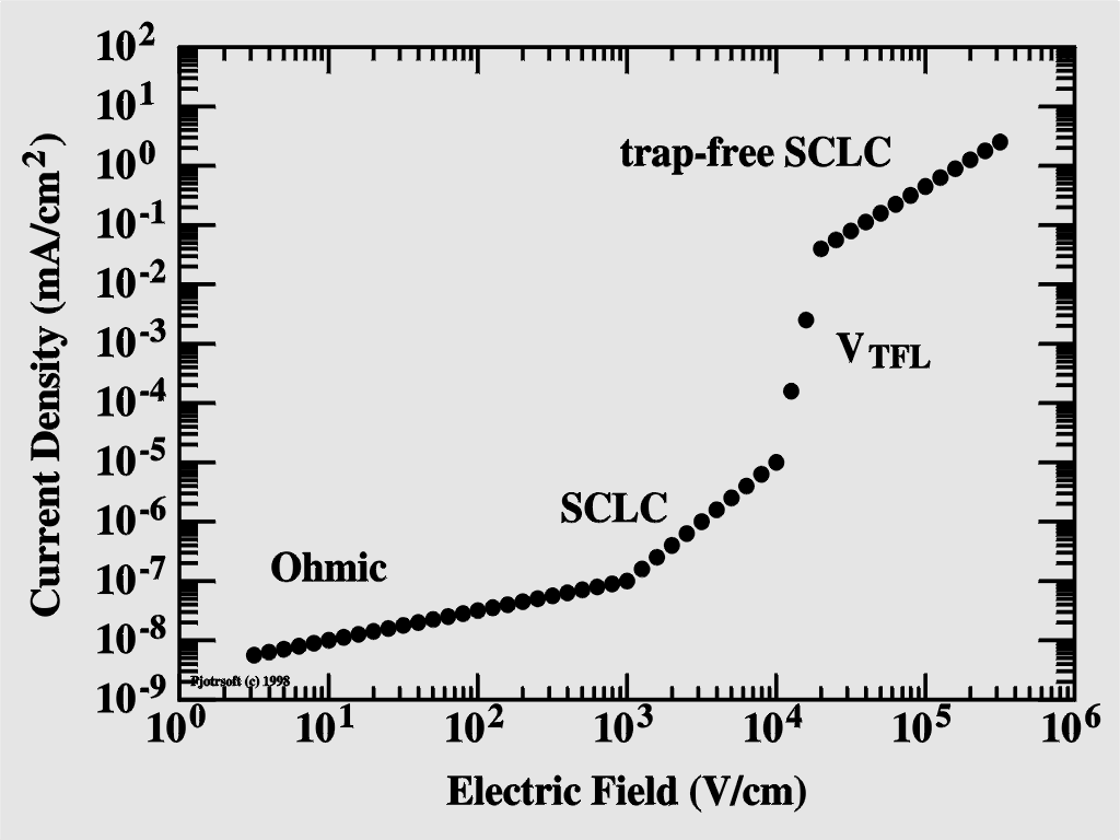 |
Ohmic: J ~ mV Space-Charge Limited Current (SCLC): Trap-Free Voltage Limit (VTFL):
Trap-Free SCLC: |
| Idisp | = |
|
= |
|
= C |
|
+ V | dC | = C | dV | + | V | dC | dV |
|
|
|
|||||||||||||
|
|
|
|
|
|
|
|
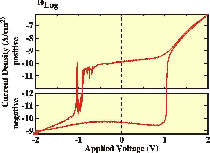
| Note that the capacitance of the device also depends on
the
voltage
(see the section on capacitance) and this
also
contributes
to the displacement current.
The figure shows an example of a large displacement current compared to the DC conductance. (Sample: PMeT/Al, 2mm electrode diameter, dV=10mV, dt=100ms, T=300K). The points where the current is zero have moved away from 0 V. For upward scanning, the displacement current is positive and the situation of zero current is reached earlier, hence the crossing point is at negative voltage. For the same reason, the zero-crossing point for downward scanning moves to the right. The obvious remedy is lowering the scanning speed. |
 |
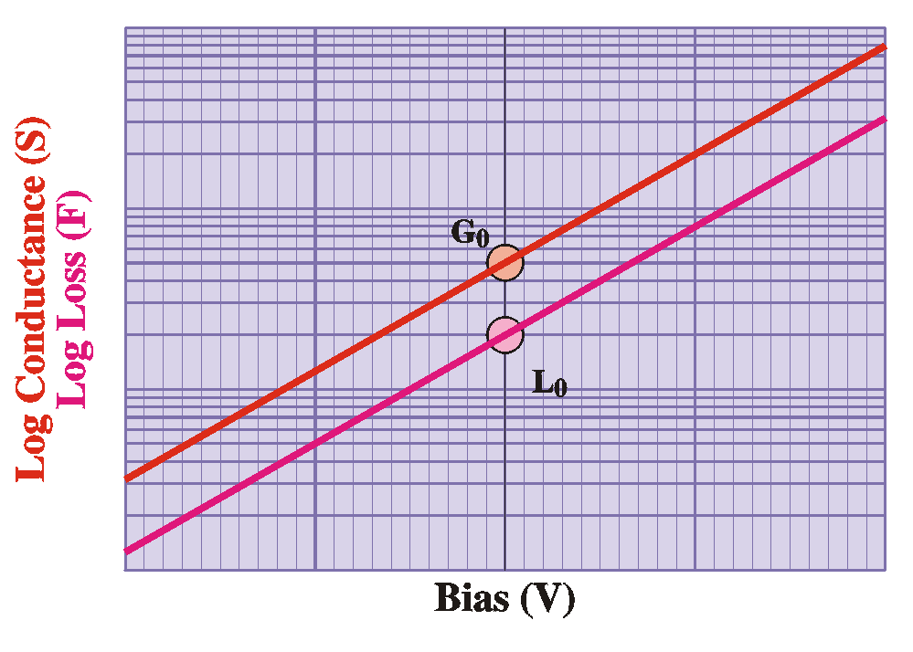
In general G depends on the applied bias (VDC) as well as the frequency (w). Later, in the section on admittance spectroscopy we will see why it depends on the frequency. On the other hand, it is easy to show why G depends on the voltage. From the previous section we have
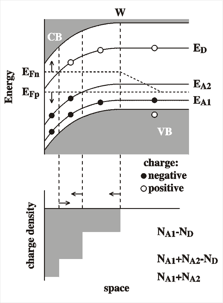 This
is visible in a sudden drop and a reduction of the slope to 1/(NA1
+ NA2) for biases smaller (more reverse) than Vbi-
(EF -EA2)/q,
as
is
easily seen in the Figure. Also, note that the apparent
built-in
voltage seems to decrease; the intersect of the slope with the
voltage
axis is lowered to Vbi-
NA2(EF-EA2)/q(NA1+NA2).
If the level is too deep and the probing frequency is too high
compared
to the characteristic level filling and emptying times
t, it does not respond anymore.
It
is still visible in a certain reduction in the slope in the
Mott-Schottky
plot, but now without the sudden drop. Important to note is
that
the slope is no longer linear and a straight-line fitting does not
reveal
the true acceptor concentration anymore; the Equation found for
the
derivative
found before is no longer valid. Also, any extrapolation of
the
local
slope to 1/C2=0 increases to beyond Vbi.
In the presence of a donor level the situation is more complex, since the position of the electron (quasi) Fermi level is not so well known. Its position is determined by the number of free electrons in the conduction band and this depends on many factors such as the mobility, concentration and life time of these minority carriers. What we can say is that the Fermi level moves in the opposite direction compared to the hole (quasi) Fermi level. When the Fermi level doesn't cross the donor level anywhere (this is most often the case, especially for shallow donor levels), the donors just act as compensation for the acceptors and a reduced acceptor concentration is found in the plots, NA -ND.
The Figure shows two simulations. In both simulations there are two levels (one shallow and one deep). In the first simulation the deep level is responding (dotted line), while in the second it is non-responding (solid line). The parameters for the simulations are given in the Table.
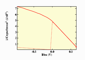
| parameter | value |
| EF | 0.6 eV |
| Vbi | 0.75 V |
| EA1 | 0.12 eV |
| NA1 | 4.28 1015 cm-3 |
| EA2 | 1.35 eV |
| NA2 | 6.272 1016 cm-3 |
| EVB | 0 eV (defined) |
| As for the frequency response, we can say the following:
For
very low
frequencies the deep states have adequate time to reach
thermal
equilibrium
at all moments and the amount of charge transferred is
proportional to
the number of deep levels and is independent of the
frequency. When the
frequency is increased beyond the relaxation time of the
levels (see
section
on emission and capture of carriers)
the amount of
charge transferred is diminished, simply because the levels
have no
time
to reach thermal equilibrium. We will measure a much reduced
capacitance
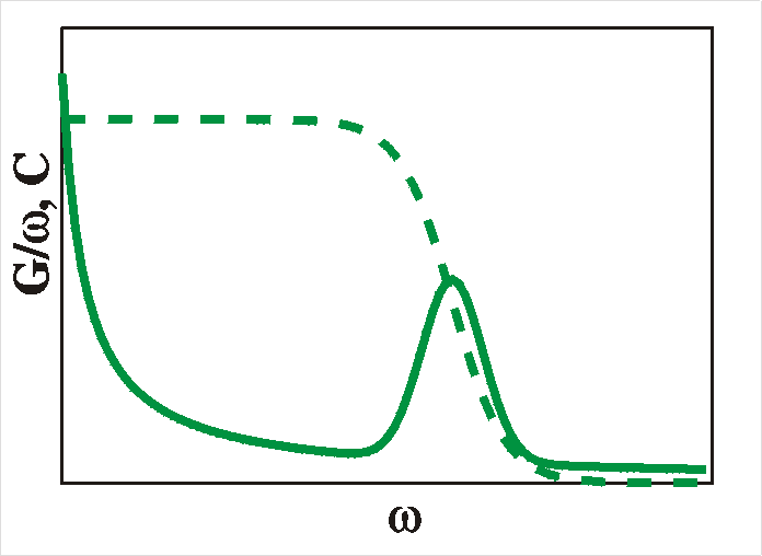
and conductance. To summarize: for deep levels we expect a bend or a drop in the CV plots and a peak in the loss-tangent (tand = G/wC) occurs when the radial frequency w is equal to the reciprocal relaxation time 1/t. |
 |

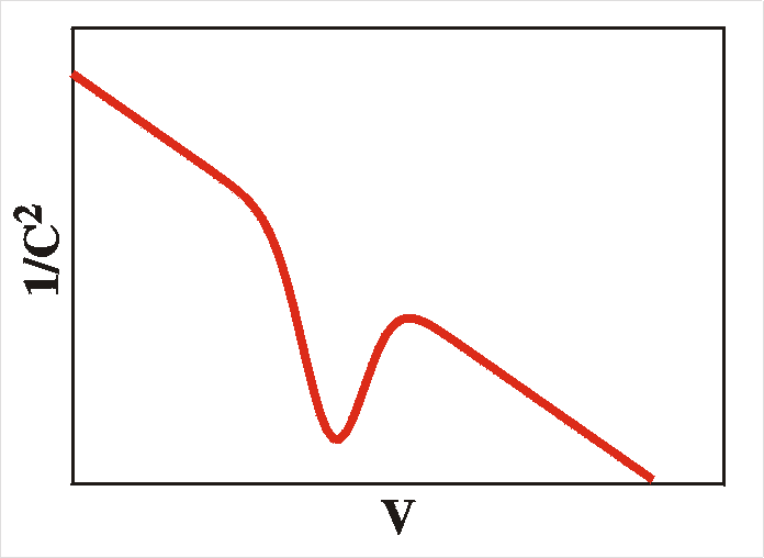
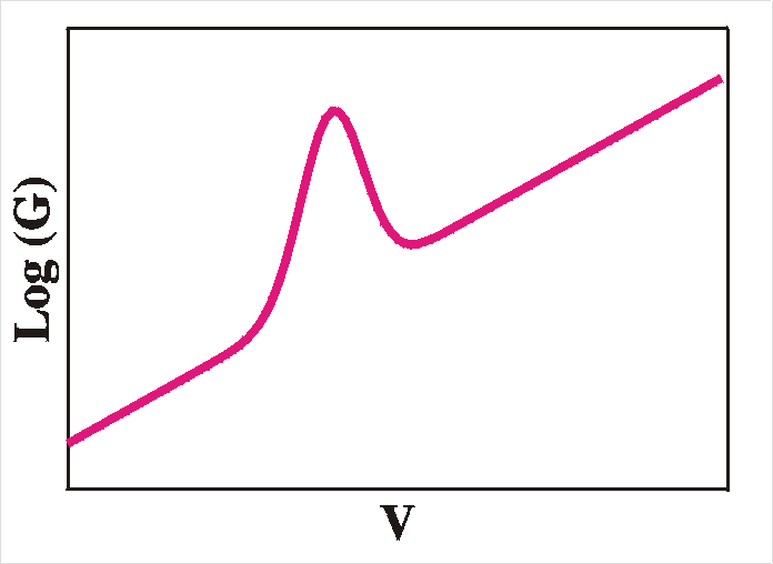
At forward bias, the Fermi level is under the interface states
and
they
are therefore empty (contain no electrons). When the bias is
lowered,
there
comes a moment where the Fermi level is resonant with the
interface
states
and they are partly filled. In that case, when the Fermi level is
modulated
(by the external bias) charge will flow into and out of the
interface
(states).
This is equivalent to a capacitance. Because energy is lost
in
the
process of moving the charges, part of the current is in-phase
with the
external voltage and is therefore observed as conductance. When
the
bias
is further reduced, the Fermi level is completely above the
interface
states
and modulating it will have no effect on the amount of charge
present
there;
no current will exist that is associated with the movement of
charge.
We
can therefore expect a peak in the capacitance-voltage (CV)
as
well
as a peak in conductance-voltage (GV), see the figure below.
 |
 |
|
|
|
To summarize: for interface states we expect a peaked response in
the
CV and GV plots and flat Cw and Gw
plots up to a certain frequency from where they will fall off
rapidly.
A maximum in loss-tangent (tand = G/wC)
occurs when the radial frequency w is
equal
to the reciprocal relaxation time 1/t.
|
|
|
|
C, G/w and tand |
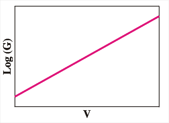
| E: single shallow level x: homogeneous |
 straight line |
 straight line |
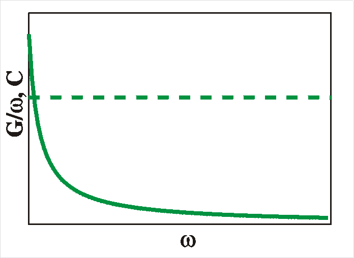 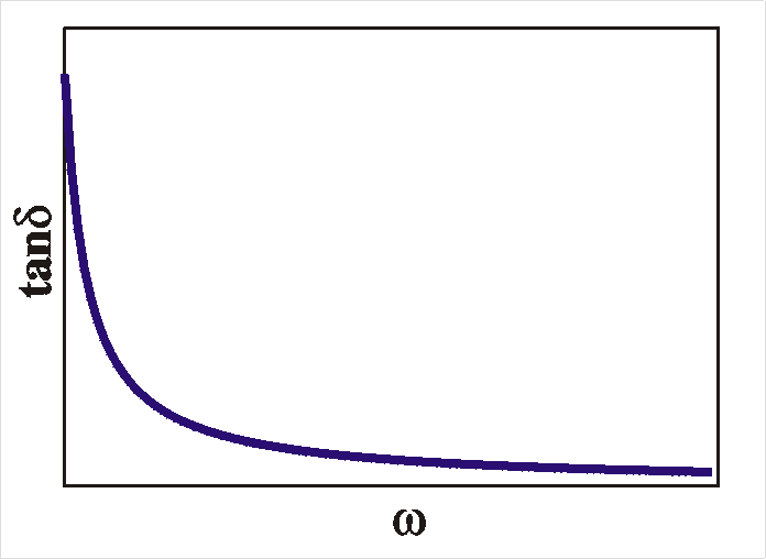 "flat" (1/w) |
| E: + deep levels x: homogeneous |
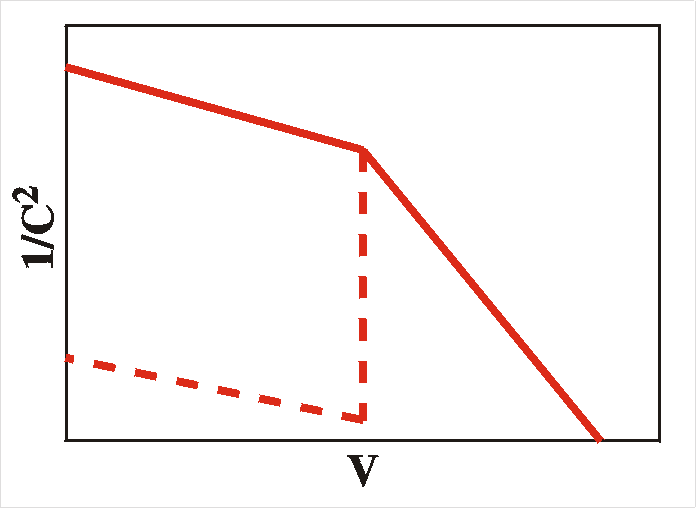 + bend or drop |
 straight line |
 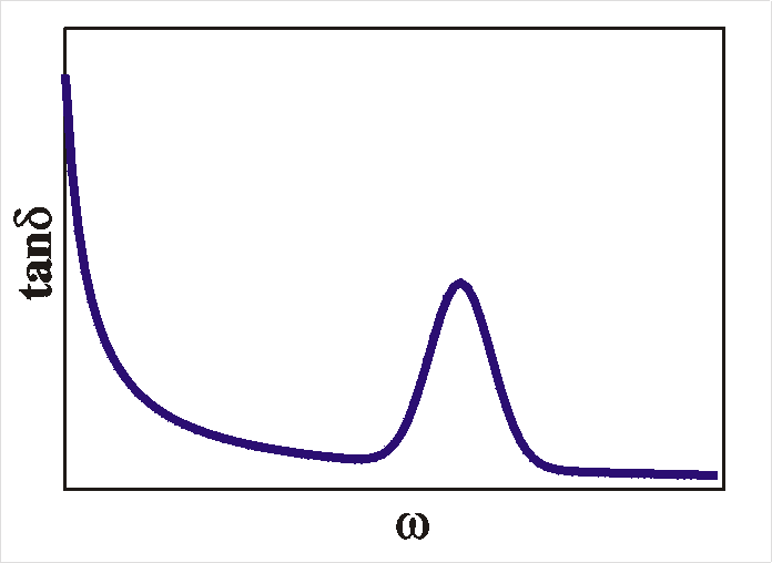 peak |
| E: + deep levels x: interface (or local) states |
 + peak |
 peak |
  peak (only at certain voltages) |
| E: + deep levels, homogeneously distributed x: interface (or local) states |
 peak (pos. depending on ac frequency) |
 peak (pos. depending on ac frequency) |
  peak (pos. depending on bias) |
Very often, the data can be described very well with
equivalent
circuits. The advantage of them is that a lot of things can be
described
in this way, but the disadvantage is that the physical meaning of
the
found
parameters is often difficult to interpret. One example of an
equivalent
circuit that is very illustrative and that still has a strong link
with
the actual physical structure of the device is the following:
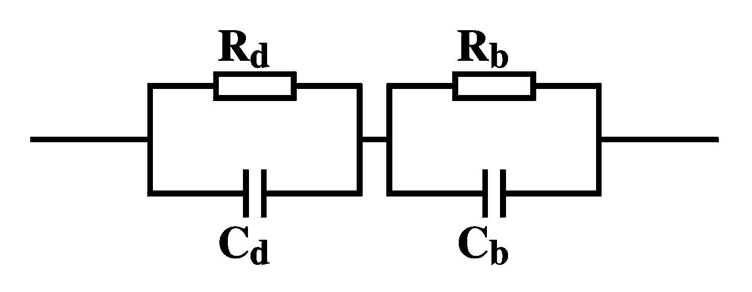 |
In the picture on the left the device is thought of as consisting of a bulk part (denoted with b) with its capacitance and resistance placed in series with the interface part (denoted with d). |
| C = |
|
|
|
| G = |
|
|
|
Under the approximations Rb << Rd and wRbRdCd2 >> 1 the loss tangent reduces to
| tand = |
|
|
|
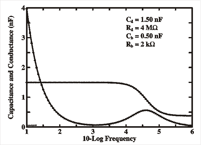
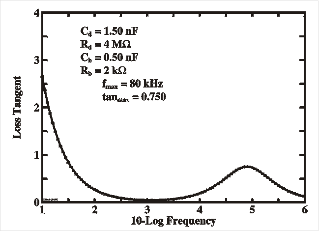
| The Figures show a simulation of the capacitance and loss (G/w) (left) and loss tangent (right) as a function of the probing frequency n (=w/2p) with the parameters as given in the Table. This resembles very much the spectra of deep levels and interface states as described in the previous sections. It is clear that for low frequencies the capacitance flattens out and saturates at the interface value Cd (assuming this is the larger of the two), while for higher frequencies it reaches the bulk value. This bulk value is in fact the so-called geometrical capacitance Cgeo which is the capacitance of the parallel plates with area A at mutual distance d filled with a dielectric medium e. |
|
|
|
|
|
|
| C |
|
|
|
| R |
|
|
|
| tand |
|
|
|
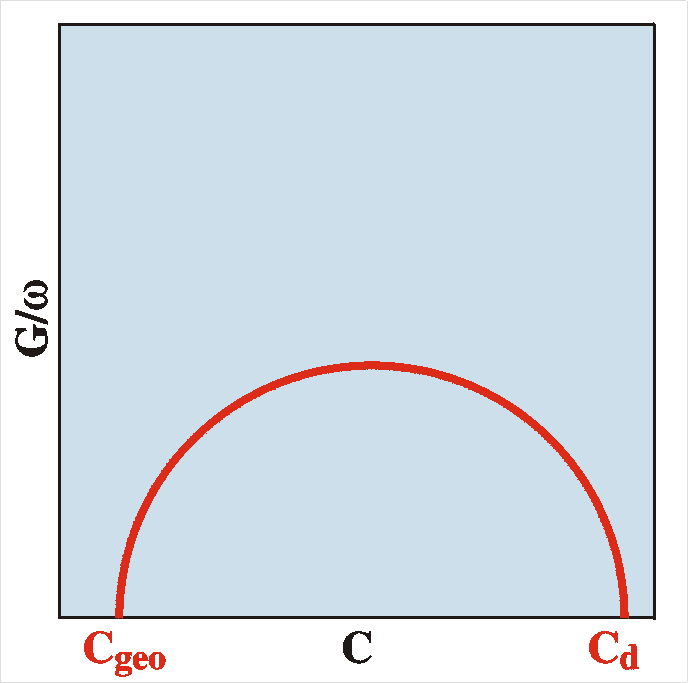
| Some people prefer to present the admittance data in the
form
of so-called
Cole-Cole plots. In that case we plot the loss versus the
capacitance.
The figure shows an example. For systems as described above
it can be
shown
that the plot is a semicircle (with the center on the
horizontal axis)
and meeting the horizontal axis at C=Cgeo
and C=Cd.
If we know the dimensions of the device, A and d,
we
can
calculate the permittivity e of
the
material:
|
 |
In the figures of the loss-tangent we see a local maximum somewhere at a frequency
| wmax = | |||
|
|
|
||
|
|
|
||
|
|
|
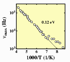 This
gives a handle for the measurement of the activation energy of the
bulk
conductance. When the temperature is changed, the bulk resistance
changes
and - assuming that the capacitances are relatively independent of
temperature
- the position of wmax
should
follow
the bulk resistance. With the assumption that the bulk conductance
is
singly
activated, the resulting temperature dependence of wmax
is
In the above theory, all parameters are assumed constants. This
is
not
a correct picture. For instance, the capacitance of the depletion
layer
Cdis
temperature and frequency dependent. A distribution of levels in
energy
will cause a frequency dependent capacitance of the form
| Cd = C0 | 1 - |
|
log |
|
||||
|
|
||||||||
|
|
|
For w=0 Cd reaches the low frequency value C0 (which is still voltage dependent), while for infinite frequencies the capacitance drops to zero. For deep levels, with t very slow, the most visible result is that the capacitance doesn't flatten out at lower frequencies. Otherwise not much changes. The position of the maximum of the loss tangent, for instance, is rather invariant to such effects.
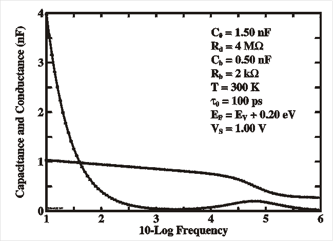
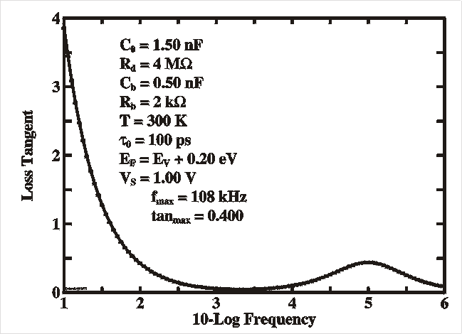
| param. |
|
param. | value | |
| C0 | 1.50 nF | T | 300 K | |
| Rd | 4 MW | t0 | 100 ps | |
| Cb | 0.50 nF | EF-EV | 0.2 eV | |
| Rb | 2 kW | VS | 1 V |
The Figures show a simulation with the same parameters as before
but
now with a frequency dependent capacitance. Note the
non-saturating
capacitance
at lower frequencies.
Some remarks:
 |
|
||||||||||||||||
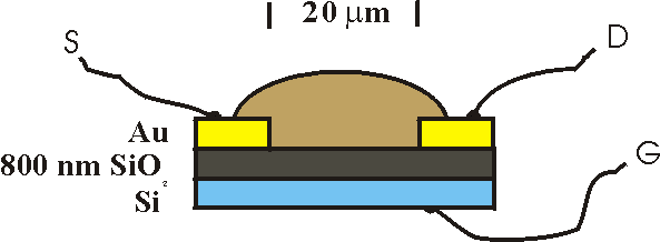
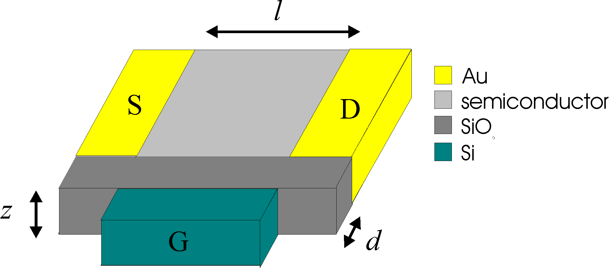
| MOSFET (Metal Oxide Semiconductor Field Effect Transistor) structure. In this case the metal is replaced by low-resistive silicon. The current from source (S) to drain (D) is controlled by the gate (G) voltage |
ID = (Z/L) m Ci [(VG-VT)VD-aVD2]
The saturation current follows the equation
 |
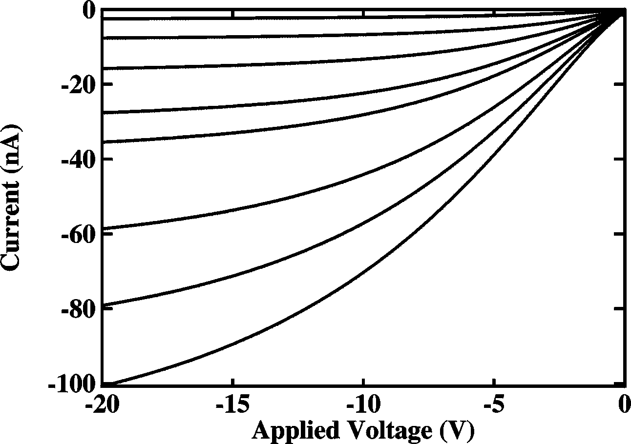 |
Here is an example: The picture on the right shows the IV plots (ID vs. VSD) of an FET for various gate-source voltages (VS=0), ranging from 0 V (top) to -35 V (bottom) in steps of 5 V. With a source (and drain) electrode length of 25 cm and distance of 25 mm and oxide thickness of 800 nm the mobility of the holes can be calculated to be 3 10-6 cm2/Vs.
Effects that we have to be aware of are
Velocity saturation. For high fields, the velocity of the
carriers
is not proportional to the field, but instead saturates to a
certain
value.
This makes that the saturation current (Ids for
Vds
> Vgs-Vt)
depends
linearly
on the gate voltage rather than quadratic (see p. 450
of Sze, ![]() )
)
Contact resistance. If we ignore the contact (or series)
resistance
at the electrodes of the device, we can underestimate the
mobility, see
Horowitz et al, JAP 1999![]() ).
).
Short-channel effects. These occur when the inter-electrode
distance becomes comparable to the depletion layer widths. In this
case,
all sorts of deviations from standard theory can occur, see
section 8.4
of Sze ![]() .
.
Other non-linear effects can make the mobility (gate)
voltage
dependent. In most cases the mobility drops for increased
gate-voltage
(Fig. 8.13 of Sze, ![]() ),
but also the opposite can happen (Vissenberg, PRB 1998,
),
but also the opposite can happen (Vissenberg, PRB 1998, ![]() ).
).
A good starting point for measuring organic FETs is the article
of
Horowitz,
"Organic Field-Effect Transistors" ![]() .
.
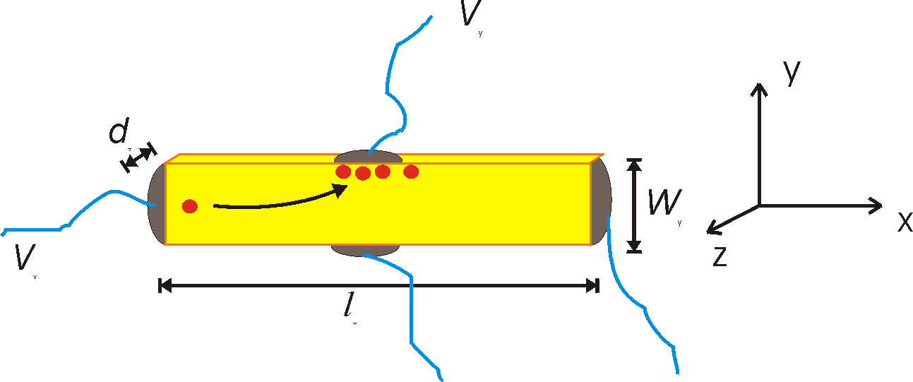 |
When we take a bar of semiconductor without any rectifying contacts we can measure its resistivity r, or conductivity s=1/r which can be expressed in terms of mobility and free-carrier density:
| mp | = |
|
|
|
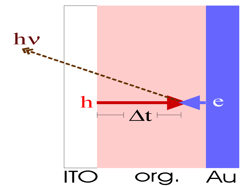
| This method is probably the most direct way of measuring
the
velocity
and hence the mobility of the carriers. With an electric
pulse,
electrons
and holes are injected from opposite sides into the active
layer. When
the carriers meet, somewhere in the active layer, they will
recombine
and
produce light. The time delay (Dt)
to
the onset of luminescence directly gives you the speed of
the fastest
carriers
(in most organic materials these are holes), assuming you
know the
thickness
of the layer (d) through which the carriers must
travel
m = v/E = (d/Dt) / (V/d) = d2 / VDt |
 |
This method is similar to time resolved electroluminescence, but
instead of measuring the light we measure the time-resolved
current on
the other side of the voltage or light pulse. The results are the
same.
Light emitting diode:
Under forward bias, majority carriers (holes from the polymer and
electrons
from the metal) are injected into the depletion region. As the
name
implies,
and as we have seen in the beginning of this document, in thermal
equilibrium
density of free carriers in this region is very low. The
injected
carriers will therefore try to recombine in a constant way
restoring
equilibrium.
The energy that is released in the process is carried of in the
form of
photons, which, if they are not reabsorbed in the material can be
detected
externally.
The energy of the photons, and hence their wavelength (read color)
is determined by the difference in energy between the holes and
the
electrons.
Holes are mostly available in the top of the valence band and
electrons
in the bottom of the conduction band. This energy difference is
therefore
equal to the bandgap. For classical semiconductors (e.g. Si) this
energy
is in the range of infra-red. For wide bandgap
semiconductors
(such
as GaN and most polymers) the bandgap is in the order of 2.5 eV
and
this
implies that the photons are in the blue part of the spectrum. A
decade
ago, the existence of blue LEDs was still a thing of the future
and
research
was focused on finding a suitable material. Candidates included
SiC,
GaN,
ZnSe, etc.
In the ideal case, all injected electrons recombine with all
injected
holes (somewhere in the middle of the depletion region) and the
quantum
efficiency is then 1, namely one photon emitted for every
electron-hole
pair injected.
It has to be noted that for an LED it is not necessary that there exists a rectifying contact. The only prerequisite is a region of low equilibrium-free-carrier concentration into which free carriers are injected. In fact, most polymer LEDs are made of ultra-pure (and hence highly depleted) semiconductor material sandwiched between two metals (often transparent ITO, indium-tin oxide) which act as electron injectors (cathodes) and hole injectors (anodes). Because there is no space charge inside the polymer there exists a linear voltage drop, instead of the quadratic voltage drop of Schottky barriers, see the figures below.
There are two ways the light efficiency might be impaired:
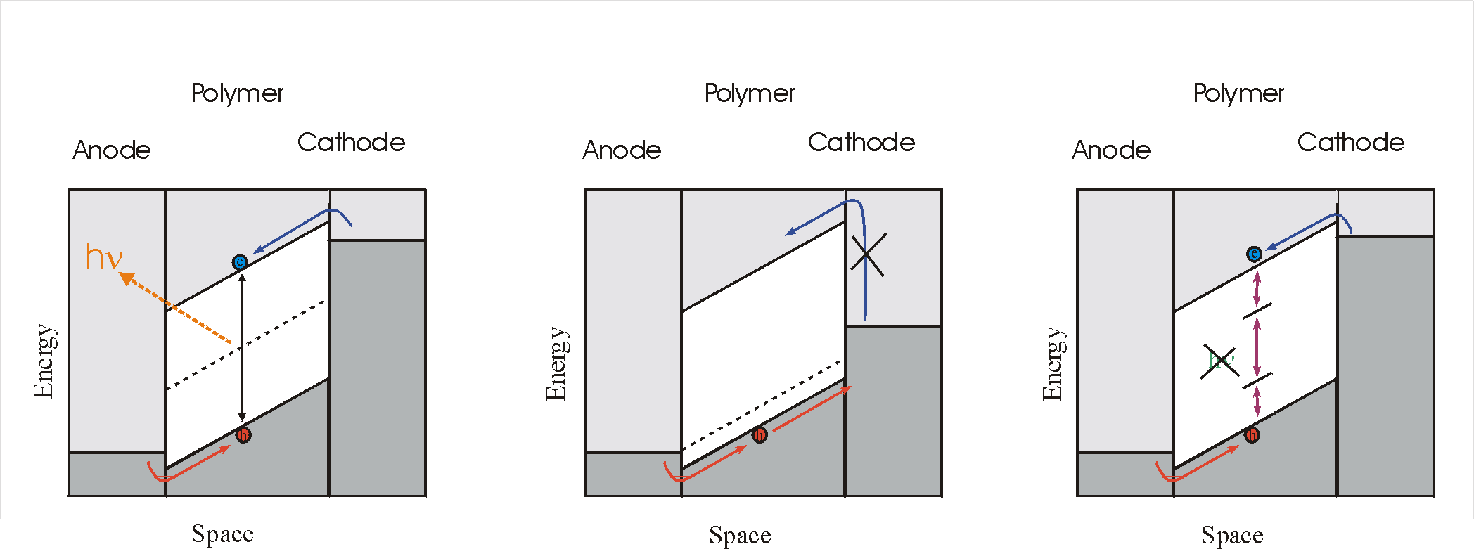
|
|
balanced injected carriers |
radiative recombination paths |
Photo-detector / solar cell:
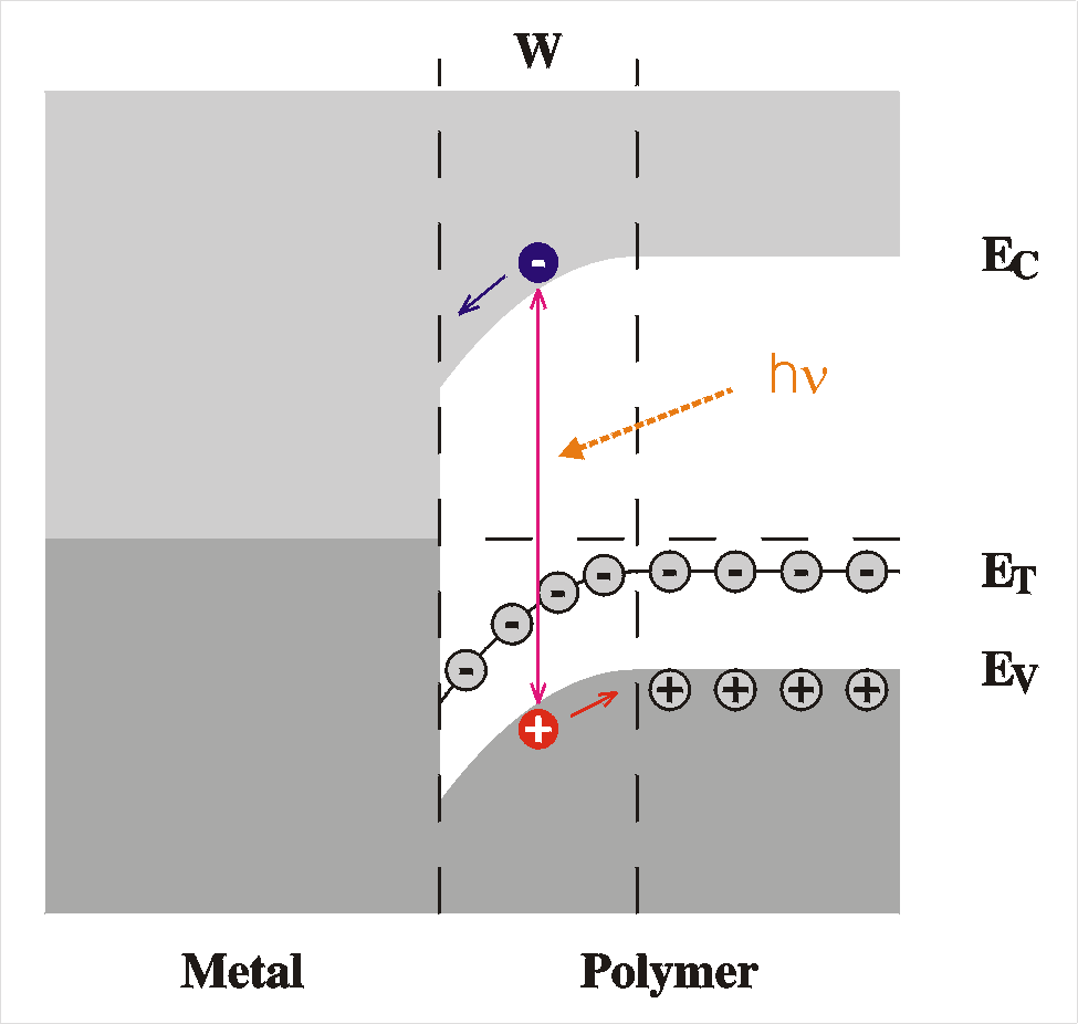
| In a photo-detector or solar cell, the opposite process takes place. The energy of photons is used in producing electron-hole pairs which are subsequently broken up by the strong electrical field in the interface. These free carriers arrive at the electrodes where they contribute to an external current. In this case, it is also not really necessary that there exists a rectifying contact. The only prerequisite is a strong electric field at the place where the electron-hole pair are formed. This field should be stronger than the binding energy of the e-h pair. At Schottky barriers such fields are easily present because the voltage drop occors over a very small length, but at sandwich structures large external voltages are needed. Moreover, no short-circuit currents are possible; The moment we short-circuit the device, the field is (nearly) gone and carriers are not separated or transported to the electrodes. Thus, while the sandwich structures are still good for photodetectors, they are not suitable for solar cells. |
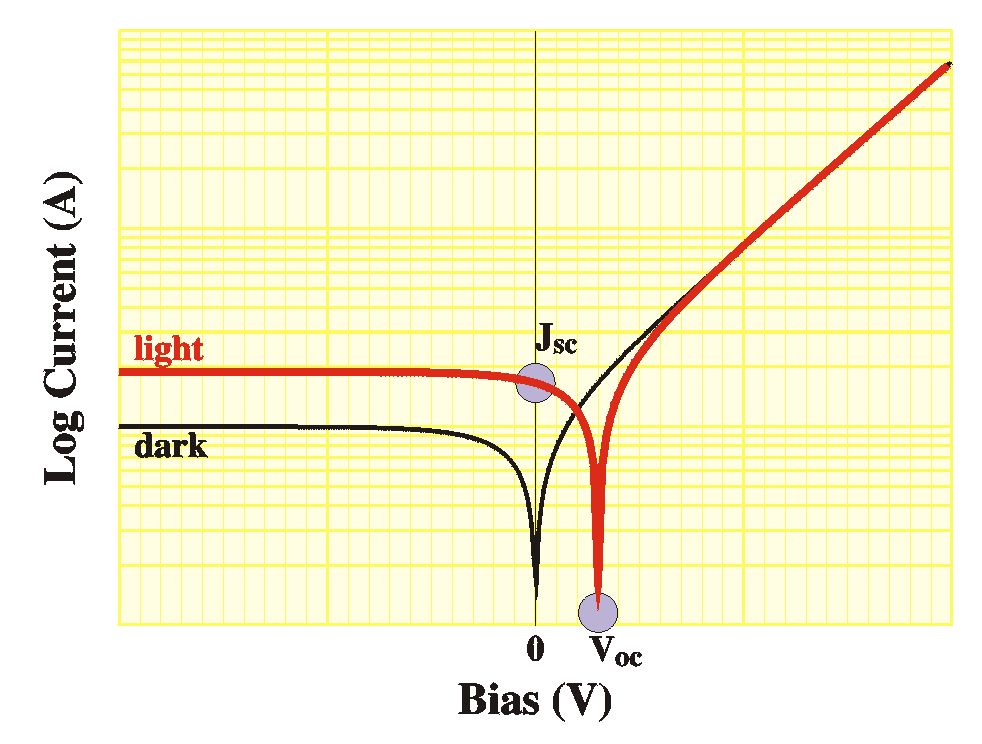
The parameters that characterize a solar cell are
 |
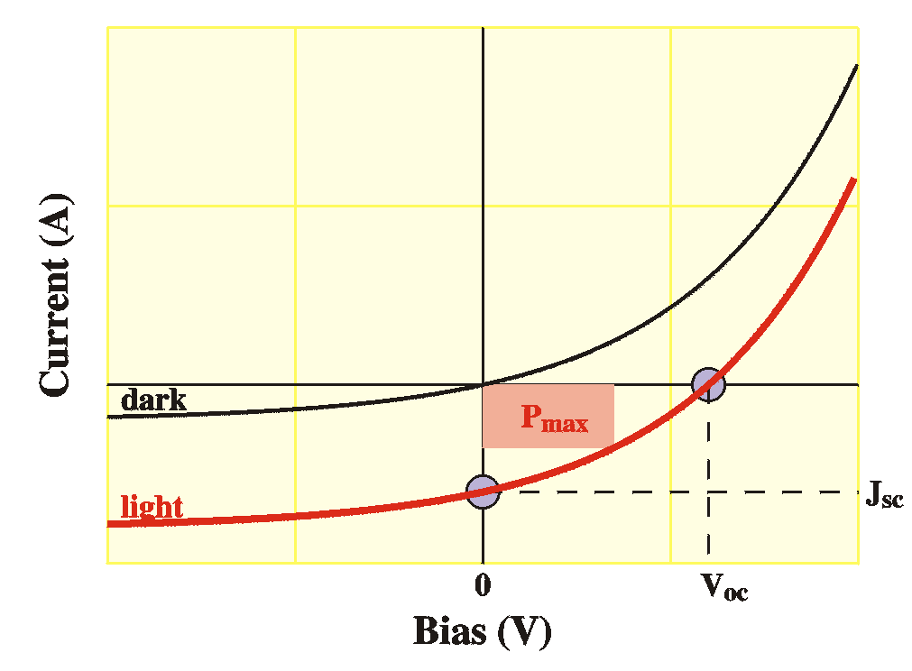 |
The figures show the IV curves in the dark (black) and under
illumination
(red) in logarithmic scale and in linear scale.
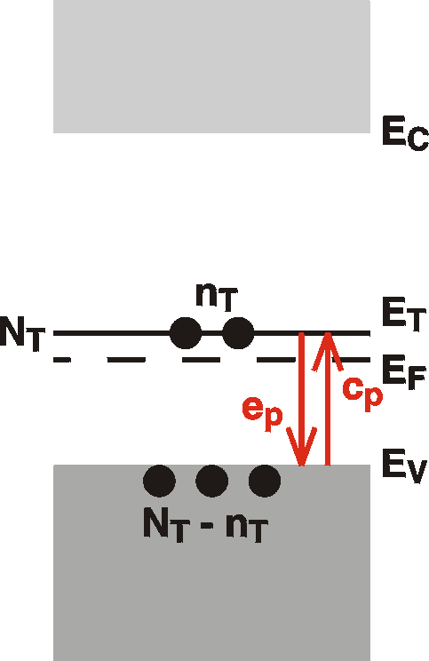 The
Figure shows the processes of capture and emission of holes from a
deep
acceptor level at ET with density NT.
The
number
nT stands for the number of levels filled
(with holes). The rest of the holes, NT-nT,
must then be in the valence band (in this simple model which
neglects a
contribution of the intrinsic holes originating from the
conduction
band).
The other numbers, ep and cp
stand
for the emission and capture rates (in units
number-per-second-per-available-hole).
The number of holes actually being emitted and captured is then
proportional
to these values and the number of available holes in the states: cp(NT-nT)
holes per second will be captured onto the trap and epnT
will be emitted per second. In equilibrium there is no net
transfer of
holes. This requires
The
Figure shows the processes of capture and emission of holes from a
deep
acceptor level at ET with density NT.
The
number
nT stands for the number of levels filled
(with holes). The rest of the holes, NT-nT,
must then be in the valence band (in this simple model which
neglects a
contribution of the intrinsic holes originating from the
conduction
band).
The other numbers, ep and cp
stand
for the emission and capture rates (in units
number-per-second-per-available-hole).
The number of holes actually being emitted and captured is then
proportional
to these values and the number of available holes in the states: cp(NT-nT)
holes per second will be captured onto the trap and epnT
will be emitted per second. In equilibrium there is no net
transfer of
holes. This requires
As seen above, the ratio of emission and capture depends on the Fermi level. We now make the assumption that the emission of holes from a trap level to the valence band is a property of the trap1. The capture of holes from the valence band is proportional to 1: the capture cross-section, sp. 2: the number of free holes in the valence band, p. 3: the average thermal velocity of these free holes, <vp>. In Equation 1:
1: we make here the assumption that the number of
available
"destination" states is infinite so that is not causing a
bottleneck in
the emission process
 |
 |
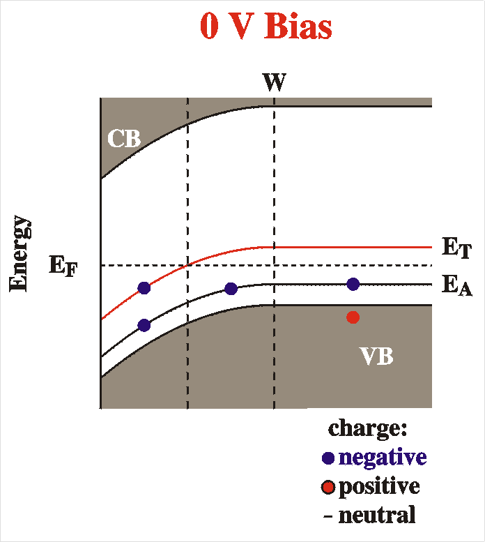
In DLTS (deep level transient spectroscopy) the capacitance is
monitored
over time after a sudden change of bias. The above figures clarify
what
happens to the capacitance after a switch of bias. Easiest is it
to
understand
if we remember that the capacitance is directly linked to the
depletion
width:
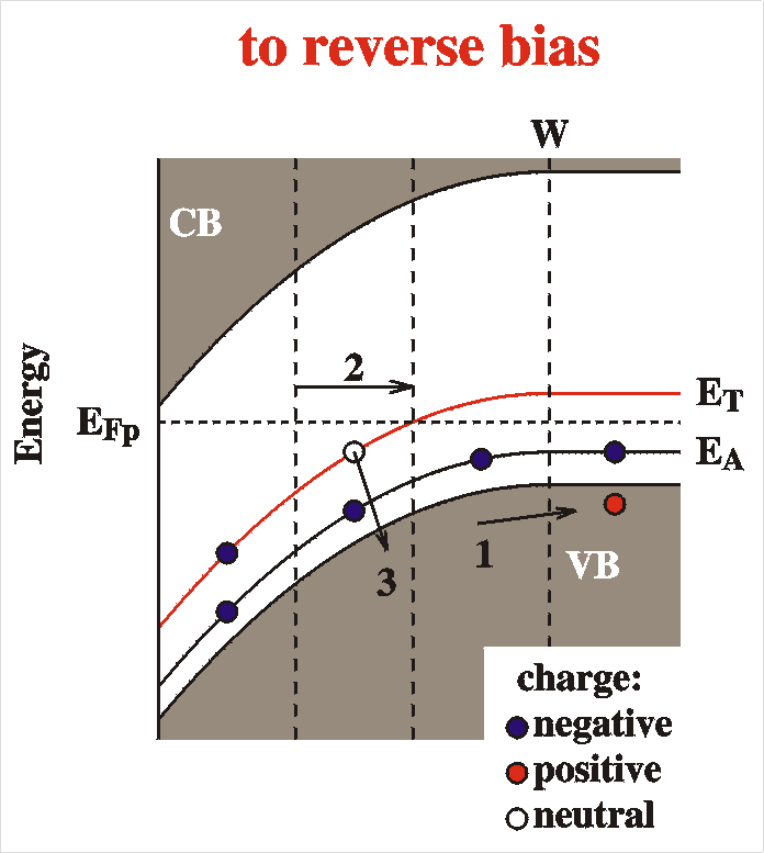
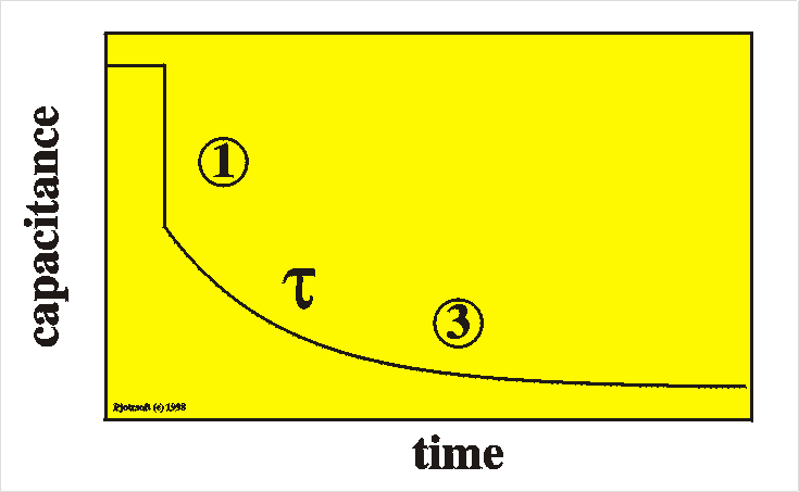
When the voltage is switched to reverse bias many things will happen. A different voltage drop Vbb occurs at the interface. This implies a new depletion width and a new capacitance according to the above equations. The new equilibrium capacitance takes time to reach. The following things will happen:
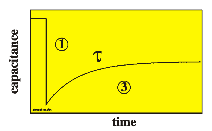 To
summarize: after a switch of the voltage to reverse bias we first
observe
an immediate decrease of the capacitance (1) and after that a slow
(partly)
recovery of the capacitance at time scale t (3).
The
explicit
form of the time dependence of the capacitance is
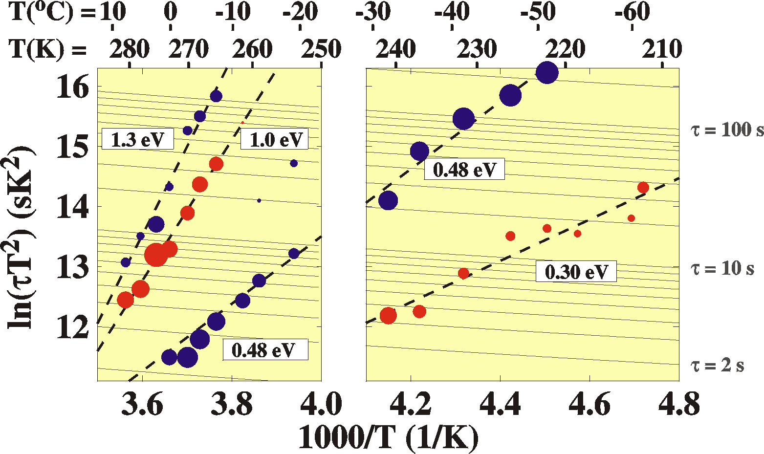
To find the trap activation energy, Epa, we can use the equation for the emission rate ep (=1/t) found in the section Emission and capture of carriers. ep = gT2spa exp(-Epa/kT). If we monitor the characteristic decay times of the transients as a function of temperature and plot this in the form ln(tT 2) vs. 1000/T, the resulting straight line will yield the activation energy.
Note: to truly measure the capacitance of the interface, Cd,
we
must
chose a frequency low enough to be below the cut-off frequency
of the bulk, see the section on admittance
spectroscopy.
For higher frequencies we would measure only the bulk properties,
which
have no transient effects.
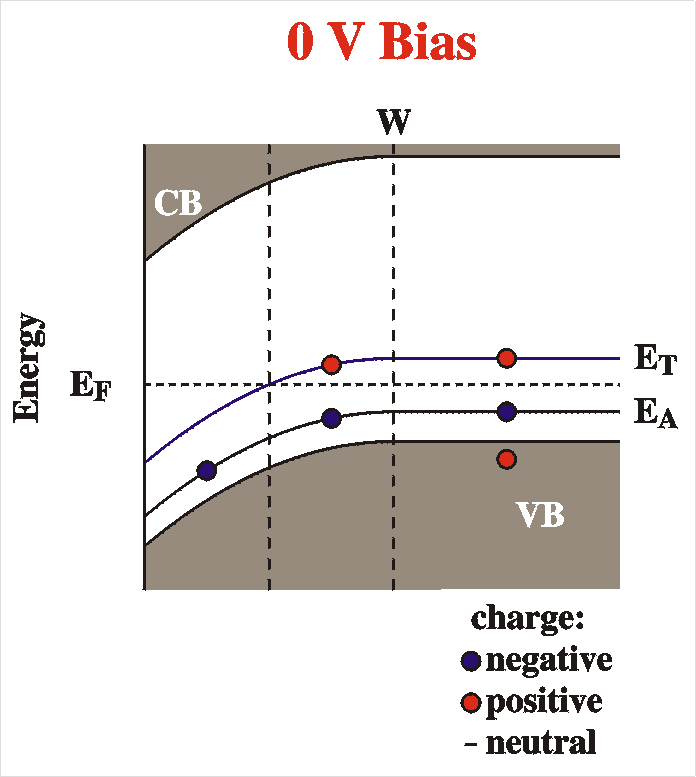
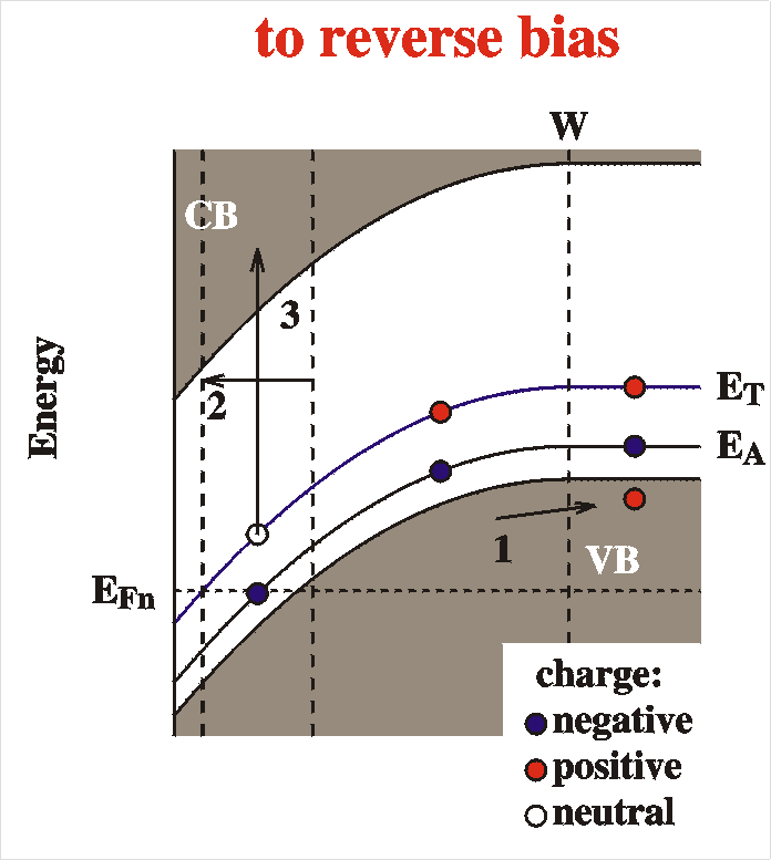
When the voltage is switched to reverse bias, the following things happen (the differences for minority carrier traps are indicated in a bold font):
 |
To summarize: after a switch of the voltage to reverse bias we first observe an immediate decrease of the capacitance (1) and after that a slow further decrease of the capacitance at time scale t (3). This is very similar to majority carrier traps, but the sign of the transient is reversed; DC is positive here. We can still determine the trap activation energy by monitoring the characteristic transient decay time t as a function of temperature. |
 |
Basic principles
How DLTS works is the following. Capacitance-transients are
recorded
in the same way as described above. The device is placed in the
emptying
voltage VE and the system is allowed to reach
thermal
equilibrium. For a short time the device is placed under the
filling
voltage
VF.
In this times the traps will fill with charges. When the voltage
is
switched
back to VE a transient is observed as described
in
the
previous sections. From this transient two samples are taken at
times t1
and t2 after switching the bias. The DLTS
spectrum
is
now the difference in capacitance at these two times as a function
of
temperature:
This means (substituting the explicit form of the transient, see the section on capacitance-transient spectroscopy)
The explicit temperature dependence of t is (see section on emission rates)
Parameters of DLTS are:
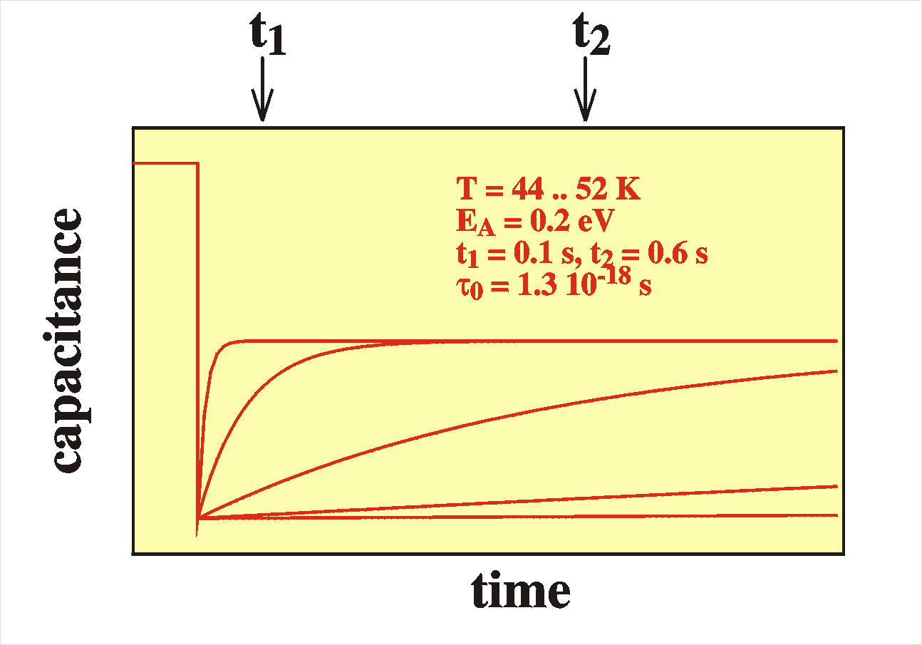 |
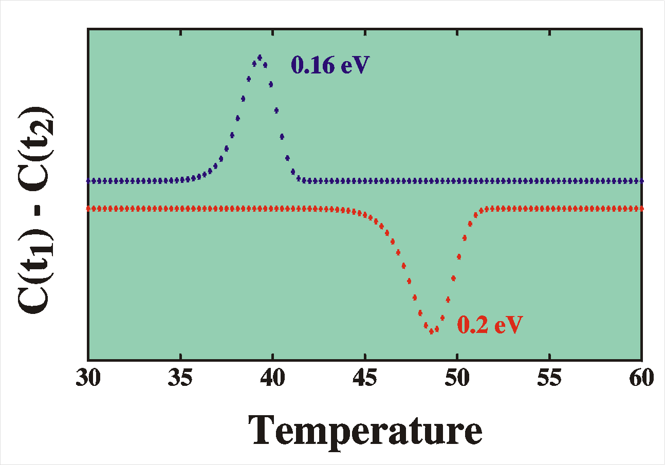 |
| Capacitance transients at several temperatures | Resulting DLTS signal for majority
traps
(down) and minority traps (up) |
Example
The Figures show a simulation of DLTS. The left figure shows
simulations
of transients caused by a 0.2 eV deep majority carrier trap for
various
temperatures (44 K to 52 K in 2 K steps). For the lowest
temperatures
the
transients are very slow (bottom trace) and the difference between
the
capacitance at t1 and at t2
is
small,
hence the DLTS signal S(T) is very small. When the
temperature
is increased the transients become faster and the DLTS signal
increases.
Note that the signal has negative sign; for majority carrier
traps, the
transient has an upward trend and therefore C(t1)
is
smaller
than C(t2). When the temperature
is
further increased, the transients become so fast that they already
died
out before the time window (t1-t2)
and the DLTS signal has vanished again. The figure on the right
summarizes
this for the majority carrier trap (red
dots;
lower
trace). In the same figure a comparison is given with a minority
carrier trap (blue dots; upper trace) whose DLTS signal
has the
opposite sign because the related transients have downward trends.
Also,
in this simulation the minority-carrier trap is chosen to be a
little
more
shallow (0.16 eV). Assuming that the pre-factor
t0
is identical (1.3 10-18 s in
both
cases) it means that the peak has shifted towards lower
temperatures.
Comments
The advantage of this scheme is that it can be done completely
automatically
with a minimum of data processing. The disadvantage is that of the
entire
transient only two points are used; most of the data are thrown
away
and
the duty cycle of the measurement is very low. In Laplace DLTS the
duty
cycle is much higher because the entire transient is used in a
Laplace
transformation. The cost is a more elaborate calculation; only
modern
computers
can be used.
In reality, DLTS is more often used not to determine the trap
activation
energies but more to show the presence of certain impurities
through
their
fingerprint spectra and to determine their densities through the
intensity
of the DLTS spectra and through the underlying amplitude of the
transients.
This is based on the fact that the amplitude of the transient is
linearly
proportional to the density of the deep defect relative to the
density
of the dopant (assuming that this ratio is small).
1: To be precise, the word spectroscopy is
misplaced,
because in a spectroscopy experiment an experimental value is
monitored
while the frequency is scanned; a spectrum is the visualization
of an
observable
as a function of frequency. In DLTS no frequency is scanned, so
the
name
is slightly inadequate. In DLTS (normally) the temperature is
scanned
and
the DLTS-signal intensity is plotted. The end plot resembles a
spectrum
in that it shows peaks and that it is a "fingerprint" of the
defect in
the material. It would have been better if "scanning" was used
for the
S in the acronym DLTS.
 |
 |
 |
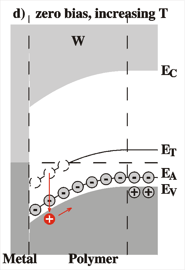 |
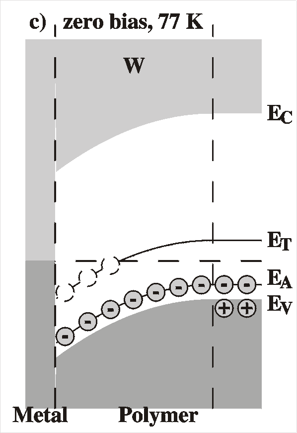
From TSC, the activation energy of the trap can be determined in
the
following way (p-type material):
In the depletion zone, there are no free carriers and the capture
of
carriers does not take place. Holes are emitted from the traps at
a
rate
ep
and the number of filled traps nt therefore
changes
with
a speed
The activation energy can also be found directly from a single TSC scan. A peak in a TSC scan follows the equation
| I = |
|
|
|
In either case, the integrated current over time reveals the number of defects emptying their charge and this can then be related to the defect density if we know the dimensions (depletion width W *and electrode area A) of the active region.
| NA = (1/eWA) | I dt |
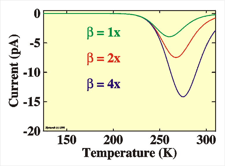
The figure shows an example of a TSC measurement with
parameters:
Ea = 0.5318 eV, A = -0.269
A,
B = 9.49 1012 (b=1x), 4.74
1012 (b=2x),
2.37
1012 (b=4x).
Note that the integrated curve (over time!) is
equal in all
three
cases. The biggest curve looks larger, but it is scanned
at higher
speed.
|
 |
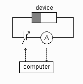 |
Setup for DC conductance (G) measurements. Setup for current transient |
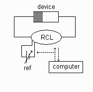 |
Setup for AC measurements of conductance (G), loss (G/w) and capacitance (C) Setup for capacitance transient |
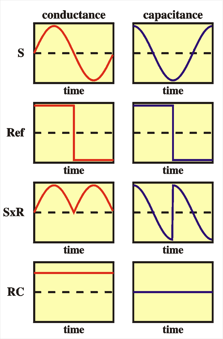
How does the RCL bridge work? In most cases it works like a lock-in detector that monitors the current when an AC voltage it applied to the device. All the current that is in phase with the voltage is interpreted as conductance (G=1/R) and the current that is out-of-phase is linked to the capacitance. This is based on the properties of resistors and capacitors, IR = V/R (Ohms law) and IC = C dV/dt. When a sine-wave voltage Vin is applied to the device, the currents for the capacitor and resistor can be calculated:
From this, the conductance can be calculated as G = I0/V
and the capacitance as C = I90/wV,
with I0 the amplitude of the in-phase current
and I90
the amplitude of the out-of-phase current. Here we made use of the
fact
that sin and cos are 90 degrees out of phase. Now the trick is how
to
decompose
the current into the in-phase current and the out-of-phase current
parts.
For this we can make use of a lock-in detector (a.k.a.
"phase-sensitive
detector"). What happens is the following:
 |
|
| device structure |
shallow level position |
shallow level density |
deep level position |
deep level density |
free carrier mobility |
conduc- tion model |
interface states |
difficulty / cost |
|
| IV | Schottky/pn bulk |
|
|
|
1 |
||||
| CV | Schottky/pn |
|
|
3 |
|||||
| admittance spectroscopy |
Schottky/pn |
|
4 |
||||||
| IV | FET |
|
2 |
||||||
| Hall | bulk |
|
8 |
||||||
| TSC | Schottky/pn |
|
|
|
3 |
||||
| DLTS | Schottky/pn |
|
|
|
5 |
||||
| ToF | bulk |
|
8 |
|
Note: the units presented here are
according
to S.I. |
||||||||||||||||||||||||||||||||||||||||||||||||||||||||||||||||||||||||||||||||||||||||||||||||||||||||||||||||||||||||||||||||||||
 page
written and maintained by Peter Stallinga,
pjotr@ualg.pt