Theory of (organic) (thin film) Field-Effect Transistors
The idea is here to present the theory of organic field effect
transistors.
I wil try to do this in a very simplified way, cutting away all the
details.
However, I am well aware that in this way, I may oversimplify
things.
This
should serve as an introduction to get a feeling for electronic
devices.
This guide does not substitute serious books like Sze and Shur,
whose
reference
can be found at the end of this document.
To explain how a field-effect transistor works, we start with a
thick-film
MOS-FET (metal-oxide-semiconductor field-effect transistor) or a
more
general
MIS-FET when the insultaor is not silicon-oxide. As we will see,
the
MIS-FET
can be well described by a MIS-diode with source and drain
electrodes
connected
in the plain of the active layer. Therefore, it is best to start
with
the
MIS juntion. Then we can extend this theory to finally arrive at
the
accumulation-channel
FET:
::: MIS junction.
::: Capacitance of an MIS junction
::: Field-Effect transistor (inversion channel)
--
Linear region
--
Threshold voltage of an inversion-channel FET
--
Subthreshold region of an
inversion-channel
FET
--
Saturation
--
Contact resistance
--
Other
contact effects
--
Stress
::: Organic FETs
--
Accumulation-channel FET
Peter Stallinga, June 2004.
MIS junction
To understand how an FET (of the MOSFET type) works, we first have
to analyze what an MIS structure is.
In a simple approximation, a MOSFET is a planar device of
semiconducting
material whose free carrier concentration n, and hence it
conductivity
(via g = men)
is
controlled
by the gate.
The first figure shows an energy diagram of an MIS device. The
device
consists of a metal and a semiconductor separated by an insulator.
Here
we assume that the insulator is not conducting any current.
Standard textbooks start with an ideal MIS device, which means
that
the Fermi levels in the metal and the semiconductor are aligned
even
before
contact. In other words, the work functions of the metal and of
the
semiconductor
are equal, fm = c
+ EC-EF.
This
implies
that we have no band bending in the absence of external voltages.
Remember
the Schottky barrier, where charge was flowing from one side to
the
other
due to the misalignement of the Fermi levels. In the ideal MIS
junction
such a flow of charge is not needed (which saves us the trouble of
explaining
how it can pass through the oxide :-)
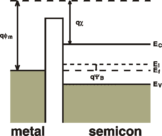 |
fm : the
metal
workfunction.
How much it costs to take an electron from the top of the
sea of
electrons
in the metal to vacuum. The "workfunction" of the
semiconductor can be
defined as c + EC-EF.
fb : (not
shown,
beause
it doesn't enter into the calculations): the barrier
height of the
oxide
as seen from the metal; the difference between the
"conduction band" of
the oxide and the Fermi level of the metal..
c : the electron
affinity of
the
semiconductor. The energy it takes to take an electron
from the conduction
band to the vacuum level.
EG : energy gap of the
semiconductor.
YB : the
energy from
the
midgap level to the Fermi level. This is approximately
equal to EG /2
EC : bottom of conduction band.
EV : top of valence band. |
| The following strip explains what happens when we
connect an
external
voltage to the metal (gate). For that we use the legenda
as shown here
on the right.
Note that the (horizontal) SCALE of the pictures is
changing.
Just like
in Schottky barriers, the depletion width depends on the
voltage. Here
the depletion width is shown as constant.
|
 |
a) Depletion
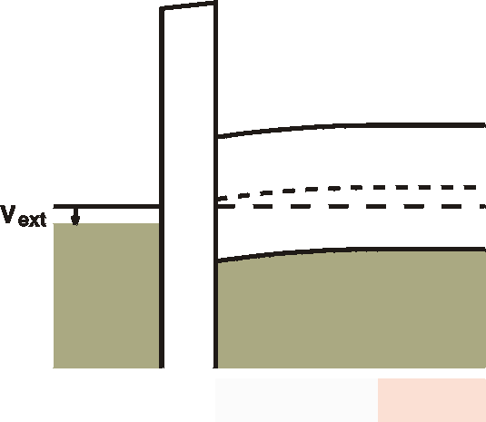 |
When a small (positive) voltage is connected to the metal
(gate), free
holes are pushed out of the interface region and a band
bending results
on the other side of the insulator. This is the same
effect as seen in
a Schottky barrier. Free carriers (holes) flow out of the
interface
region
and a depletion zone is formed. The uncompensated
(negatively)
ionized
acceptors cause an electric field and - via Poissons
equation - a
parabolic
bending of the bands.
Note that there is also a voltage drop in the oxide. In
the oxide no
charges can reside and hence the field is constant and the
voltage drop
is linear in space. The total voltage drop in the oxide
plus the band
bending
is equal to the external voltage. |
b) Inversion
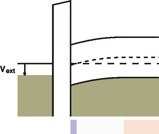 |
When the voltage is further increased, at the interface an
inversion
region is created. The semiconductor becomes here n-type,
albeit not
very
conductive, yet. |
c) Strong Inversion
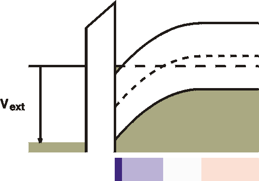 |
For very strong bias, the Fermi level crosses the
conduction band close
to the interface. This is strong inversion. Free
electrons are
in
a so-called "channel" next to the oxide. This channel is
therefore
highly
conductive.
The ample availability of states in the conduction band
means that
further increases in the gate voltage will not extend this
strong
inversion
region into space, but rather will increase the density
of
electrons
in the channels. The channel is always infinitisimally
thin.The huge
amounts
of free carriers can easily cause a large voltage drop
(band bending)
and
only a thin layer is needed to "absorb" the external
voltage.
Note that the depletion width (the white zone) and the
inversion width
(lightblue zone) are constant once the channel is formed. |
d) Accumulation
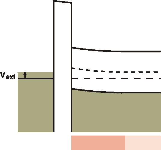 |
Going in the other direction, a negative voltage at the
gate metal
will attract some free holes to the interface. In this accumulation
region, an increased number of free holes is created,
although it is
not
yet dramatic; the interface is still high-ohmic. |
e) Strong accumulation
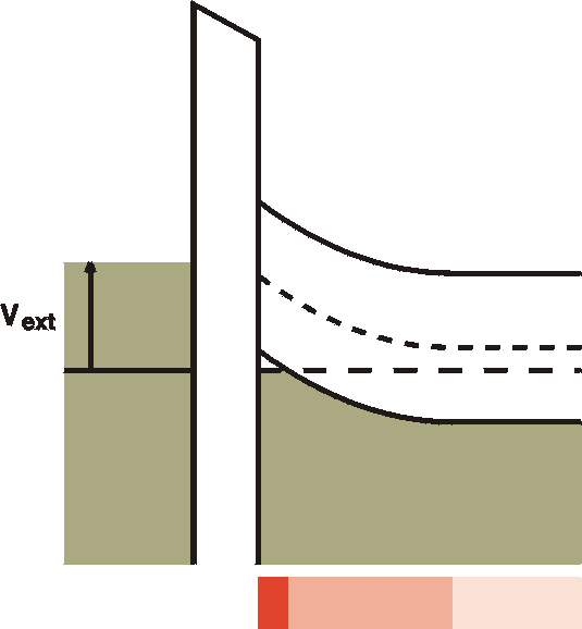 |
For stronger negative voltages at the gate the Fermi level
is forced
below the valence band at the interface. A channel with
high density
free
holes is created. This is called strong acummulation.
Again, as for the strong inversion case, further
increasing the voltage
will result in an increase of the density of the free
holes rather than
an increase of the channel in space. In the picture the
width of the
channel
is exaggerated. In reality it is only a monolayer thick. |
To complete the story, in strong inversion we have the
following
distribution of space charge and free carriers:
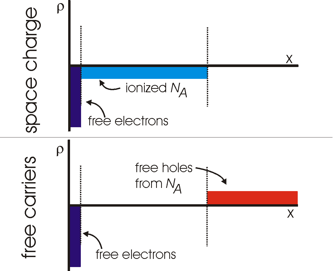 The MIS junction is an ideal device for studying interface states
and
deep
levels using the same techniques as demonstrated for the Schottky
barrier.
The advantage lies in the fact that there is no DC current which
might
obscure our measurements.
The MIS junction is an ideal device for studying interface states
and
deep
levels using the same techniques as demonstrated for the Schottky
barrier.
The advantage lies in the fact that there is no DC current which
might
obscure our measurements.
Capacitance of an MIS junction:
The device can consist of several regions in series, each with it's
own
capcitance. The capacitance of the metal and of any part of the
semiconductor
with free carriers is zero. For the other two parts of the device,
the
insulator and the depletion region we can calculate:
Cox = eox
/
d
CW = es
/
W
The total capacitance is caluclated by taking the serial sum of the
capacitances:
|
Cox x CW
|
|
| depletion: Cd
= |
----------- |
accumulation:
Ca = Cox |
|
Cox + CW |
|
In acuumulation there is no depletion layer and in this case, the
total
capacitance reduces to Cox. Once a depletion zone
is
formed, the capacitance depends on the frequency. For low
frequencies,
the generation-recombination current causes a short circuit of the
depletion
capacitance and the capacitance reduces to Cox.
See
Fig.
7 on p. 371 of Sze  or Fig. 4-3-5a on p. 348 of Shur .
For high frequencies, the depletion zone is not short circuited and
the
measured capacitance is a series capacitance of the oxide and the
depletion
width. The depletion width is constant once it is fully formed (see
images
above) and we will measure a constant capacitance.
or Fig. 4-3-5a on p. 348 of Shur .
For high frequencies, the depletion zone is not short circuited and
the
measured capacitance is a series capacitance of the oxide and the
depletion
width. The depletion width is constant once it is fully formed (see
images
above) and we will measure a constant capacitance.
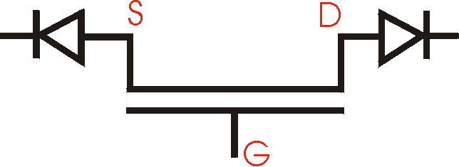
Field Effect Transistor (FET)
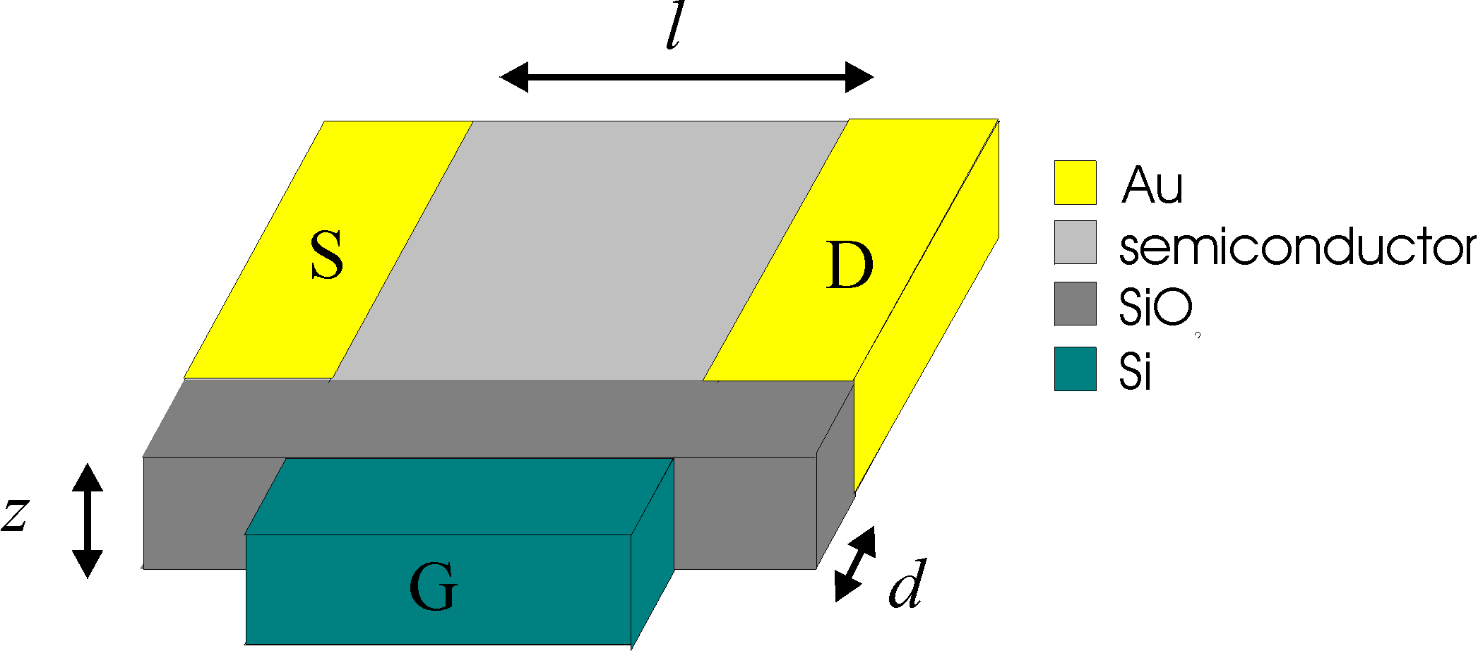 |
Directions:
x: from oxide to surface of film
y: from source to drain
z: along an electrode
Z: electrode width
L: electrode distance
d: oxide thickness
|
An FET is nothing more than an MIS device with electrodes connected
on
two lateral sides of the semiconductor. Imagine connecting an
electrode
above and one below the images above. The first one we will call the
source,
the latter the drain.
The total current through this device is then linearly
proportional
to the number of free carriers in the semiconductor. The other
parameters
are the mobility m, the external
electrical
field Ex: and the device dimensions Z and
L:
IDS =
Z|Q|mEx
=
Z|Q|
mVy/L
(
I )
with IDS the total current, m
the mobility of the carriers, Vy the external
voltage
(is equal to VDS), Z the width of an
electrode,
L
the distance from source to drain, and |Q| the amount of
free
charge in a line perpendicular to the oxide surface (along
x) in
C/m2. This is equal to integrating the electron and hole
density
(ignoring the sign) from the edge of the oxide to infinity (or to
the
limits
of the semiconductor film), see the figure with free carriers above.
In case we have substantial contributions from both electrons and
holes, and they have different mobilities, we have to replace the
part
|Q|m with (|Qp|mp
+ |Qn|mn).
We will see that this can explain the linear region of an FET. To
calculate
the IV curves in the linear region, we only have to calculate the
number
of free carriers. For the saturation region the equations are a
little
different, as will be shown later.
Linear region
As a first order we can say that we only have free carriers when we
are
in strong inversion or strong accumulation. As can be seen from the
strip
of figures above, we need to supply a certain voltage to the gate to
induce
either strong inversion or strong accumulation.This is the so-called
threshold
voltage VT. This doesn't mean that we don't have
free
carriers and conduction below this threshold voltage, but that the
conduction
beyond this voltage is much larger.
Under the assumption that all the free carriers come from charges
in
the strong accumulation or depletion zone, it is very easy to
calculate
the amount of charge on the semiconductor side and hence the
current.
In
the section above we have seen that the capacitance of an MIS
junction
under these conditions is equal to the oxide capcitance, Cox.
Assuming no other capacitances, all the charges go to the
interface and
therefore, since C = Q/V we find Q
=
Cox VG. As written
above,
we need VT to bring it into strong accumulation
or
depletion,
therefore Q = Cox
(VG
-VT).
With this in mind, and with the idea that the conduction is
proportional
to the charge as seen in equation I the current in the linear
region
becomes
IDS
= Cox
(VG -VT)
mVDS Z/L
|
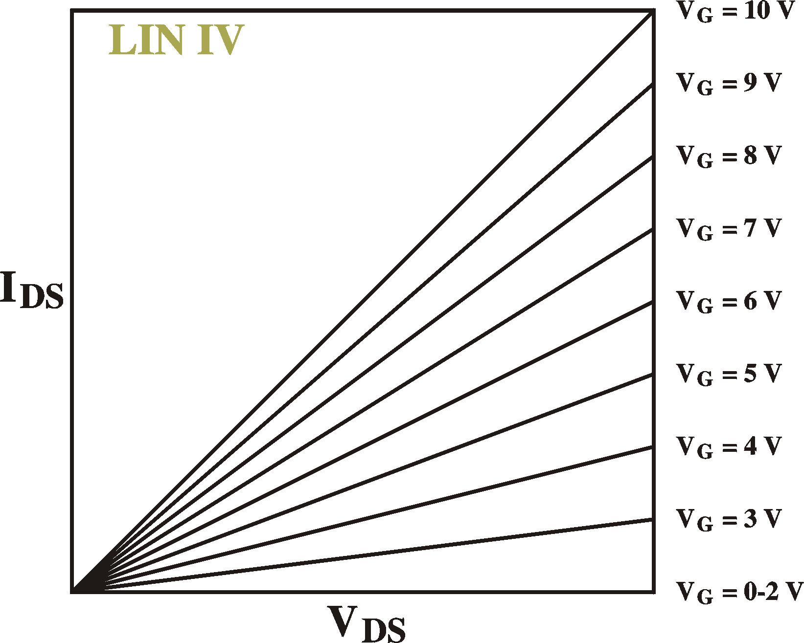
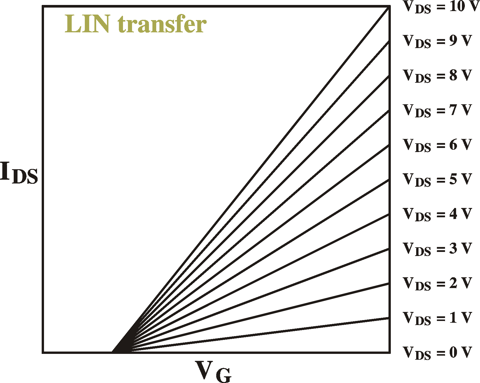
Examples of IV curves (IDS vs. VDS;
left)
for different gate voltages and transfer curves (IDS
vs. VG;
right) for different drain-source voltages. VT = 2 V.
Remember that we arrived at this by the assumption that all the
free
carriers are located in the strong inversion or accumulation zone
close
to the interface and that the rest of the device is not
conducting.
Especially
in materials with bulk Fermi levels close to the band edges, the
background
conductivity (the "off current") can be very large. In principle,
the
purer
the material, the closer the Fermi level will be to mid gap and
the
less
off-current we will have. Making the films thinner also helps.
Moreover, not all the charge induced by the gate is free charge.
The
above model is also known as the Charge Control Model. If we do
include
the background conduction in the bulk and the depletion and
inversion
zones,
we have to add a term to the above equation, to arrive at the
Schottky
model, see Sze
and Shur .
Threshold voltage of an
inversion-channel
FET
Following the above discussion and the MIS strip of figures, it is
clear
that the band bending cannot be larger than the bandgap before
either
strong
accumulation or strong inversion occurs. In other words, at the
onset
of
strong inversion, the band bending Vbb is exactly
equal
to the difference between the conduction band and the Fermi level, (EC-EF)/q
in the bulk.The depletion width is then (see section on Schottky
barrier)
W
= (2esVbb/
qNA)1/2.
The electrical field at the interface is the integral of the space
charge
inside this depletion region: Emax = (qNA/es)W
= (qNA2Vbb / es)1/2.
Maxwell's equations tells us that, in the absence of any charge, the
displacement D (=eE) is
continous
accross the interface. On the semiconductor side of the junction we
have
Ds
= es(qNA2Vbb/
es)1/2.
In the oxide we therefore have an electrical field of Eox
= (1/eox)(qesNA2Vbb)1/2.
This field is constant inside the oxide because there are no net
charges
there. We therefore have an extra voltage drop of DV
= doxEox = (dox/eox)(qesNA2Vbb)1/2
accross the oxide. The total external voltage then becomes (dox/eox)(qesNA2Vbb)1/2
+ Vbb = VT.. With Vbb
equal to (EC -EF)/q
this becomes
VT = (dox/eox)[2qesNA(EC-EF)/q]1/2
+ (EC-EF)/q
Remember that Cox = eox/dox,
and, in normal cases, the Fermi level is very close to the valence
band,
so that (EC-EF)/q
= EG/q which we can call 2yB.
With this in mind, the above equation becomes the following text
book
equation
for an n-type inversion channel:
VT
= (4qesyBNA)1/2
/ Cox + 2yB
|
As an example: for NA = 1x1016 cm-3,
Cox
= 50 mF/m2,
EG
= 2.5 eV (yB = 1.25 V), es
= 5.0e0 we get VT
= 11.9 V + 2.5 V = 14.4 V; since the first term in the equation
comes
from
the oxide and the second term comes from the semiconductor we can
see
that
most of the external voltage (83%) is absorbed by the oxide
(remarkably).
The Fermi level, of course, also depends on the acceptor
concentration,
so in total we get a complex dependence on NA.
In
textbooks,
it is assumed that all acceptors are ionized. In fact, for organic
materials,
where the acceptor level can be very deep (but abundant) this is
not
necessarily
the case. In fact, we should read NA as
"ionized
levels"
and this can be a fraction of the real number of acceptors, unlike
in
classical
materials such as Si and GaAs. Moreover, the fraction of levels
ionized
can be changed by changing the band bending (by applying a gate
voltage)
and thus, the threshold voltage can change when putting the device
in
operation.
Depending on the depth of the levels, these changes can be in the
order
of seconds, to minutes and hours and even days.
Note that high levels of current have no effect on this trapping
of
charges, since they do not attribute to a different band bending
or
extra
charges in the interface.
Note that for an accumulation type FET this calculation does not
work
because we do not have a space-charge region caused by ionized
acceptor
levels; VT does then not depend on NA.,
but
only on the Fermi level and the number of valence band states.
Remark: We have considered here an FET without a wire connected
to
the
bulk of the device. If we do so, the threshold voltage reduces to
VT
= (2qes(yB-Vsub)NA)1/2
/ Cox + 2yB,
with
Vsub
the voltage of the substrate.
Subthreshold region of an
inversion-channel
FET
The subtreshold region is the region of gate voltages before the
channel
is opened. The desnity of free carriers at the interface is
exponentially
depending on the distance between the conduction band and the Fermi
level.
When the channel is formed, the Fermi level remains fixed (resonant)
at
the edge of the conduction band. Further increases in voltage result
only
in a tiny shift of EF; only minute changes in EF
are needed to create free charges Cox(VG-VT).
In the subthreshold region the distance EF-EV
is determined by the gate voltage and the acceptor concentration in
the
bulk in the following way (very similar to the calculation of the
threshold
voltage above):
1) Poisson's equation tells us that the band bending in the
semiconductor
is equal to double-integral of the density of ionized acceptors: Vbb
= double-integral NA
2) This will tell us the field at the interface and hence
3) The field and voltage drop in the oxide and hence the
4) Total voltage drop in the device.
5) Reversing these calculations, if we know the total voltage
accross
the device, we will also know the band bending in the semiconductor.
6) If we know the band bending in the semiconductor and we know the
initial distance between Fermi level and conduction band, we will
know
the position of the Fermi level at the interface.
7) If we know the position of the Fermi level at the interface, we
know the density of free carriers at the interface (Fermi-Dirac
distribution,
which is more or less exponential)
If you do the calculation correct, you will see that the distance
of
the Fermi level depends linearly on the gate voltage and with a
square-root
on the acceptor density NA. Hence the current
follows
something like (Sze ,
Szur )
Ids
= I0
exp[VG /  NA]
NA]
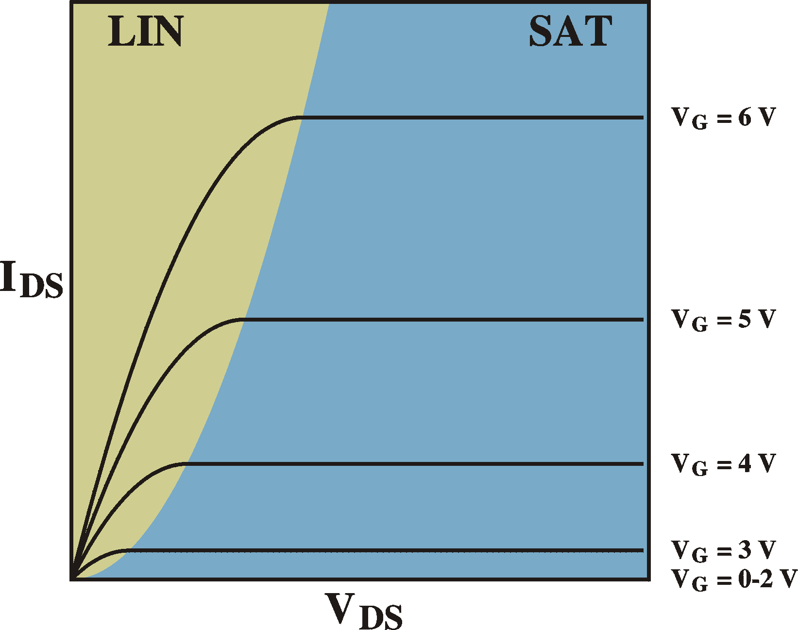
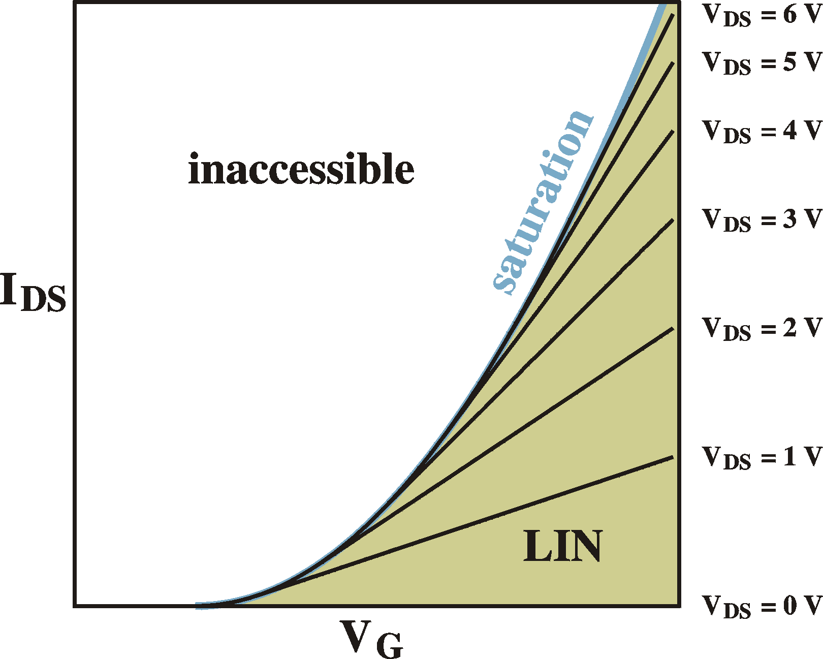
Saturation
If we increase the drain-source voltage eventually we will go into
saturation
where the current becomes independent of the drain-source voltage It
is
very easy to understand why this should happen. Imagine an FET with
a
threshold
voltage of VT = 1 V. We will apply a gate voltage
well
beyond this value, let's say 10 V. The channel is therefore open.
For
low
drain-source voltages, both the drain and the source and hence the
entire
bulk region of the device is at 0 V, or close to 0 V at all places.
At
the drain, the gate-drain voltage is 10 V and this is well beyond
the
threshold
voltage. Here we have a conducting channel. At the source (which is
always
at 0 V), the gate-source voltage is also 10 V and here the channel
is
also
open. Actually, at all places do we have a conductive channel.
Let us now set the drain voltage to 10 V. At the source we still
have
a gate-source voltage of 10 V and the band bending here will still
induce
a channel. However, at the drain, the gate and the drain are at the
same
voltage; the gate-drain voltage is 0 V and this is below the
threshold
voltage for creating a conductive channel. The channel is closed
here.
This we call pinch-off.
If we assume a linear voltage drop from source to drain from 0 to
10
V, we can exactly calculate where the channel closes, namely at
10%
distance
from the drain. We have to bear in mind, though, that a closed
channel
has less free carriers and thus has higher resistivity. The law of
continuity
tells us that the current at every place of the device must be
equal.
Therefore,
since voltage drop is current times resistivity, the voltage drops
much
faster in a closed-channel region than in a open-channel region.
Moreover,
if we assume that the free-carrier density in the closed-channel
region
is much smaller than the open-channel region, the pinch-off region
is
very
small.
The voltage of start of saturation is easy to calculate. At this
voltage
the gate-drain voltage is exactly equal to the threshold voltage.
VG-VD
= VT. Thus (VS = 0, VD
= VDS)
onset of saturation: VDS = VG-VT
Beyond this voltage, the current is constant. We will have a
region
from the source to near the drain with a voltage drop of VG-VTand
a very thin region close to the drain with the rest of the voltage
drop
of VDS. The length of the first region is nearly independent of
the
total
external voltage. It therefore has a contant length and voltage
drop,
and
the current through it is therefore independent of
VDS.
Again, continuity tells us that the current at every point is
equal,
therefore,
the saturation current is independnet of VDS.
With this we can calculate the free carrier density Q(x)
and the voltage V(x) of every point in the channel
at
the
onset of saturation. Along the way we will also calculate the
current
which
is the current in saturation.
Imagine putting up a screen at a distance x from the
source,
peprpendicular to the source-drain direction, stretching as long
as the
electrode lengths (Z) and as high as the film thickness. We can
calculate
the current I through such a screen.
The current I at a crossection at a certain point x
is
equal to the free-charge density at that point Q(x),
the
carrier mobility m and the local field
E(x)
= dV(x)/dx:
I(x) = ZmQ(x)
dV(x)/dx
Because of continuity, this current has to be constant along x
and equal to the drain-source current IDS. The
above
equation then reduces to
dV(x) / dx = IDS/ZmQ(x)
(eq.I)
The free-carrier density is a function of the local field VG-V(x),
as seen before:
Q(x) = Cox[VG-V(x)-VT]
(eq.II)
The solution to this system of diferential equations is easy (take
the derivative of the second equation and put this in the first),
to
which
we add the following boundary condition:
1a: the charge at the drain is zero: Q(L)
= 0.
1b: The voltage at the drain is just enough to
close
the channel: V(L) = VG-VT.
 The
soulution is then The
soulution is then
Q(x) = [(2CoxIDS/Zm)(L-x)]1/2
V(x) = (VG-VT) - [(2IDS/mZCox)(L-x)]1/2
Using the next boundary condition
2a: The voltage at the source is 0: V(0)
= 0
2b: The charge at the source is Q(0)
= Cox
(VG-VT)
we can calculate the current |
IDS
= (1/2)m(Z/L) Cox
(VG-VT)2
|
which is the current at the onset of saturation and,
since,
as
we have shown before, the current beyond this point is independent
of VDS,
this is the current in saturation (as long as VG
< VDS + VT).
The total amount of charge stored in the device in saturation can
be
found by integrating the equation for the charge distribution
above and
multiplying by the device width Z:
at saturation, VDS = VG-VT:
Q = (2/3) Z (VG-VT)
Cox
in the same way:
at VDS = 0 V
:
Q = Z (VG-VT)
Cox
Note: when we increase the bias, charge is coming out of the
device.
We have to be careful in our IV measurements that we do not
measure the
current of these charges going into and coning out of the device.
See
the
section on displacement current.
We can also use the same method to calculate the current before
saturation.
Going back to the general solution of the system of differential
equations:
V(x) = (VG-VT)
-
[(2IDS/mZCox)(x0-x)]1/2
As boundary conditions we now take:
1: The voltage at the source is 0; the charge
is
Cox
(VG-VT)
2: The voltage at the drain is V(L)
= VDS
The result is
IDS
= m(Z/L) Cox
[(VG-VT)VDS
-
(1/2)VDS2]
|
which is equal to what we found for the linear region,
except
for
the term VDS2 which becomes important
only
when we approach saturation. When we susbtitute VDS
<<
VG-VT
we get the equation for the linear region. When we substitute the
saturation
condition VDS = VG-VT
we reproduce exactly the equation for saturation currents.
Examples of IV curves (IDS vs. VDS;
left)
for different gate voltages and transfer curves (IDS
vs. VG;
right) for different drain-source voltages. VT = 2 V.
For completeness sake and for later reference, here are the
charge
distributions
and voltage curves for the different regimes, ranging from 1)
equilibrium,
2) linear regime, 3) onset of saturation, 4) in saturation.
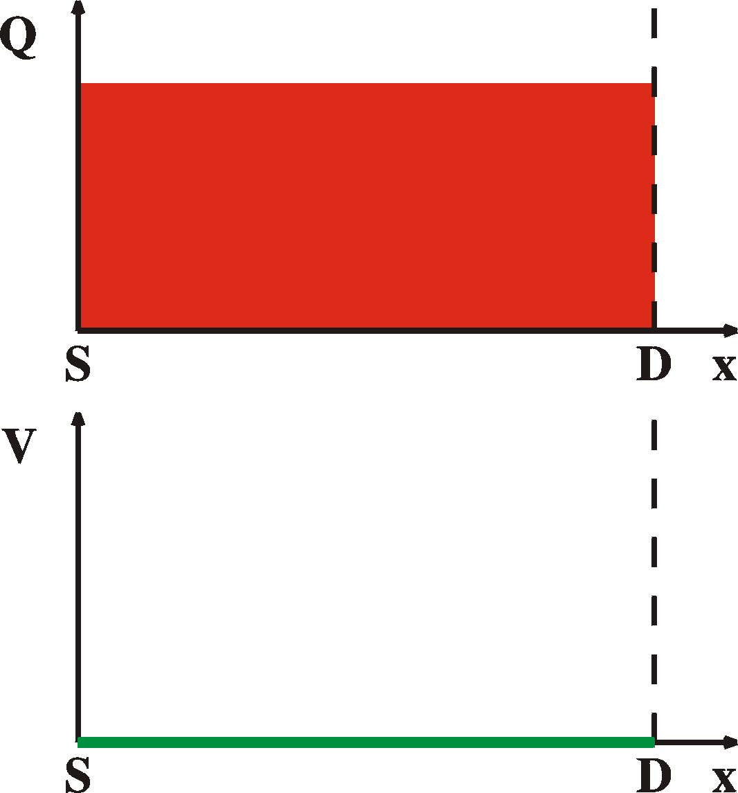
|
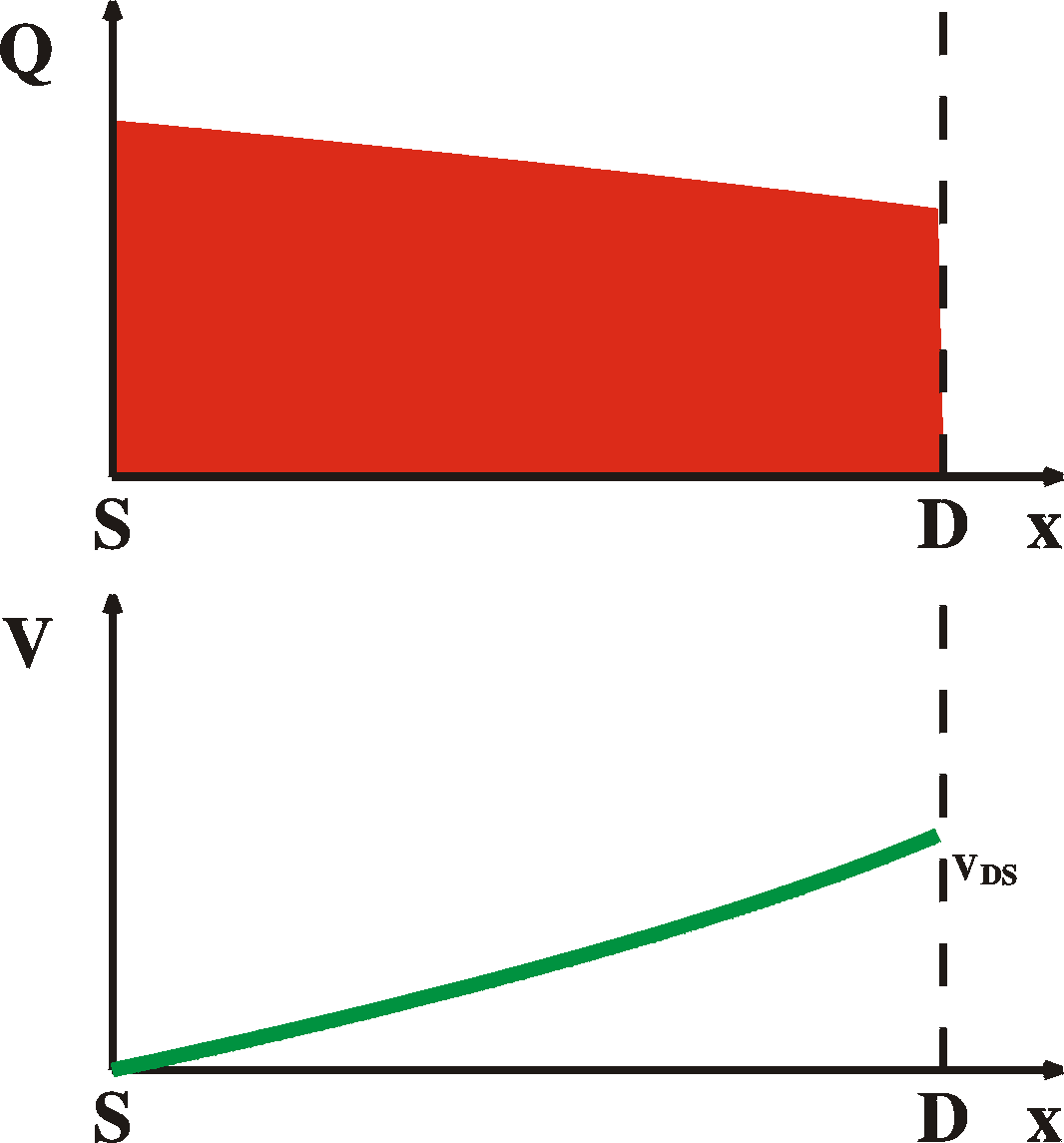
|
|
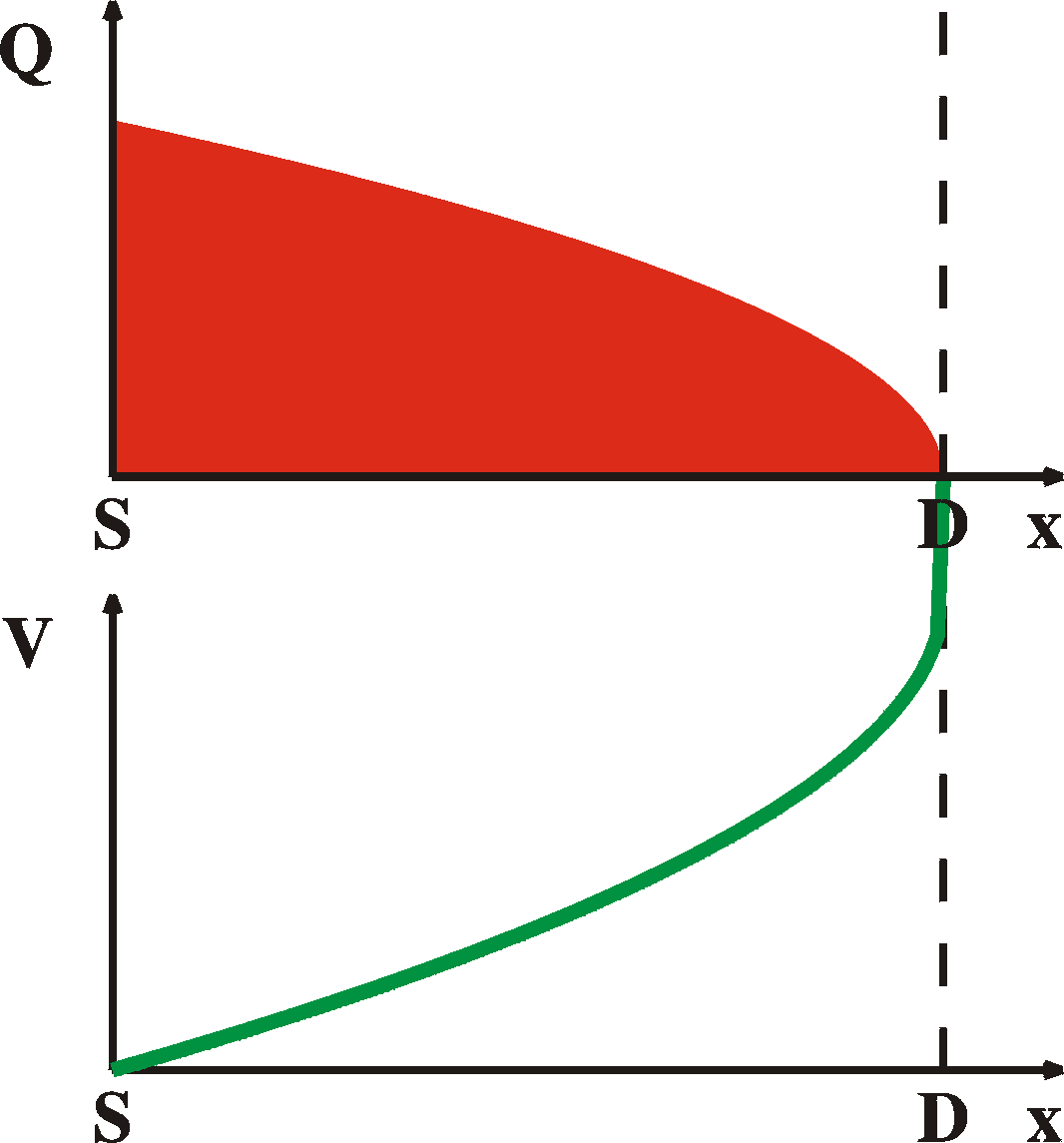
|
|
VDS = 0 V
|
VDS < VG-VT
LIN
|
VDS = VG-VT
onset of SAT
|
VDS > VG-VT
SAT
|
Contact resistance
In the above discussion it was assumed that the injection of carrier
is
not a limiting factor. In other words the contacts were considered
low-ohmic
However, the contacts can cause a severe barrier for the injection
of
carriers.
The most obvious one is when at the electrodes a high-resistive
region
is formed. This causes the current to grow sub-linearly in the
linear
region.
This can easily be shown in a simulation.
For strong currents, the contact resistance can become the limiting
factor and the current saturates and becomes independent of VG:
We have to imagine that the FET is made up of two contact
resistances (2Rc)
and the channel resistance, connected in series. Initially the
current
grows linear with VG (as explained by the text
above).
The channel resistance is thus proportional to 1/VG.For
large
VG the channel resistance disappears and the
current
settles at VDS / 2Rc.
More exact: when the current is increasing, the contact resistance
induces a voltage drop at the source, Vs = Ids*Rc,
the field at the source (Vgs) is reduced and the
current
drops (external observables in bold):
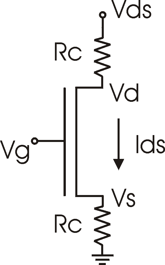 |
Vs = IdsRc
Vd = Vds
- Ids Rc
Vgs = Vg-Vs
Ids =
mCoxZ/L (Vgs
-VT)
(Vd
-Vs ) |
Simulation
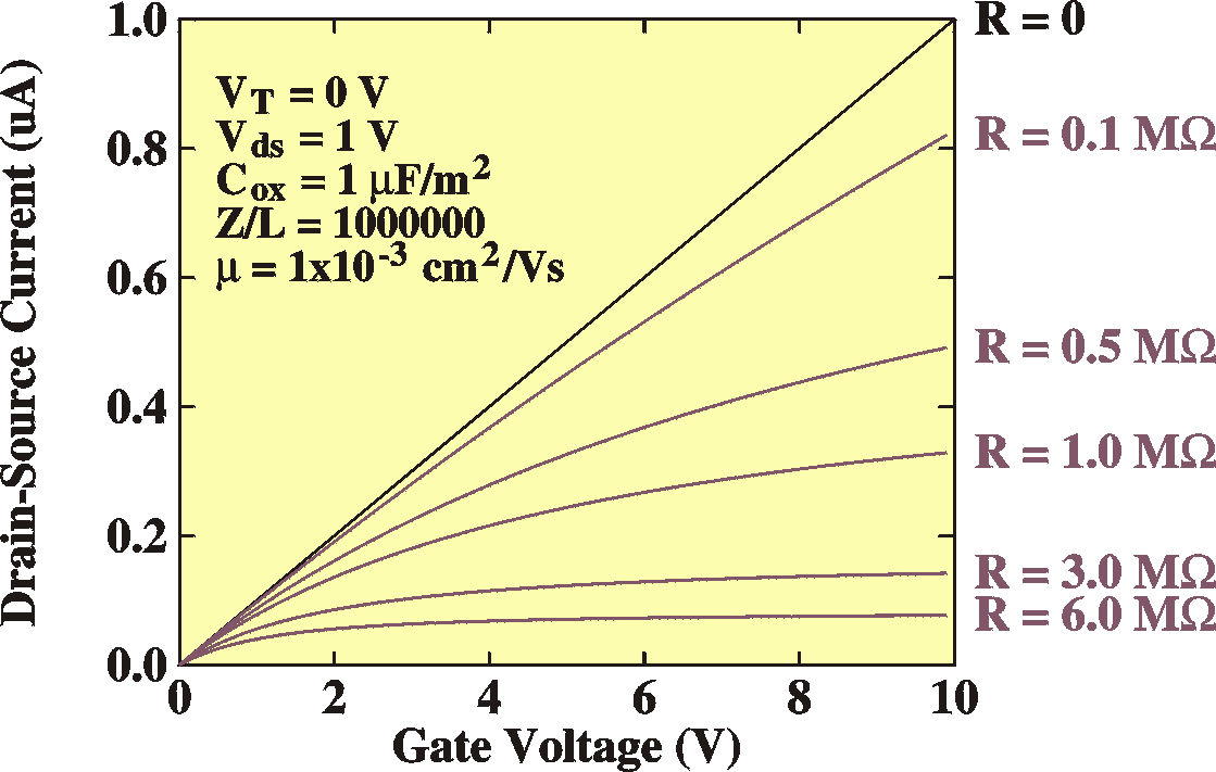
Transfer curves
|
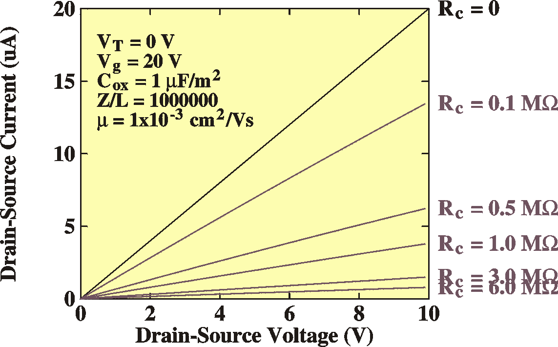
IV Curves
|
Other contact effects
The interface regions are not necessarily ohmic, as described above.
Contacts
are normally made of metal and the contact of this metal with a
semiconductor
might result in a Schottky diode. When a depletion layer is formed
between
the electrodes and the semiconductor, the current, might be limited
by
this Schottky barrier, see the bipolar
device theory pages. However, these effects can be easily
minimized
by chosing a suitable electrode material. Normally, gold makes a
good
low-ohmic
contact with p-type organic semiconductors.
In case the devices do have depletion regions at the electrodes, one
side effect of this is that the saturation region doesn't saturate.
This
is especially pertinent for short channels, where the size of the
depletion
regions can be comparable to the channel length. Remember that the
depletion
width depends on the bias. In this case the bias is the drain-source
voltage.
When the bias is changed, the depletion width is changing. The
channel
(the rest of the distance between drain and source not filled by the
depletion
zone) is changing and the current can change, even in the saturation
region.
In the extreme case, the depletion zones of the source and the drain
can overlap. In this case, the entire area between the source and
drain
is depleted and we enter the space-charge-limited current regime.
Stressing; threshold voltage shifts upon
time
Stressing is the efffect that the threshold voltage VT
changes with time when the bias is applied. It is not so difficult
to
imagine
how this can occur:
As shown above, the current is linearly proportional to the density
of free charges (Ids = a Qfree).
These
free
charges are induced by the gate voltage and grow linear with VG
once the threshold voltage has been overcome, Qfree
=
Cox(VG-VT).
In
other words, part of the gate voltage is not used to induce free
carriers,
but only serves to polarize the device and induce band bending.
After the free charges have been induced in the channel, they can be
trapped onto deep localized states (Qfree becomes
Qtrap).
In these states they do no longer contribute to the current, while
they
still contribute to the induced charge: Qfree + Qtrap
= Cox(VG-VT).
The
current therefore drops. Moving Qtrap to the
other
side of the equation, it is easy to show that effectively VT
increases:
Ids = a Qfree = Cox[VG-(VT
+ Qtrap/Cox)]
Effectively, the threshold voltage has increased by Qtrap/Cox.
In other words, we have to apply a larger bias to maintain the same
current.
The evolution of VT and Ids
depends
on the dsitribution of the trap states. In most cases the traps are
not
at discrete energy, but have a wide distribution. The currents drop
therefore
in a non-exponential way. Empirically, the best fit is obtained with
(Stallinga
2004 )
Ids= Ia exp[(t/t)a]
+ I0
The threshold-voltage shift is best described by a so-called
stretched
hyperbola (Gomes 2004 )
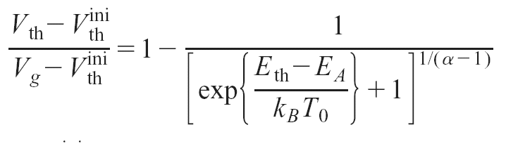 with Eth = kBT ln(nt).
Organic FETs
Why doesn't this (always) work for our organic materials?
|
|
The organic FETs are of the accumulation p-channel
type. In
the accumulation operation there is no space charge region
caused by
uncompensated
ionized acceptors. All the space charge and band bending
must come from
intrinsic carriers - unbalanced holes-electrons which still
follow pn
= NCNVExp(-EG/kT),
but
p>n - and carriers in the strong
accumulation
channel.
The result will be that we will still have the equations
IDS = Cox
(VG -VT)
mpVDS Z/L
IDS = (1/2)m(Z/L)
Cox
(VG-VT)2
for currents through the strong accumulation channel in the
linear and
saturation regions, but that the threshold voltage doesn't
follow the
same
equation anymore as given before.
The threshold voltage now becomes (see Horowitz )
VT = qNA/Cox
However, see the chapter below about accumulation
FETs. |
|
|
The FETs are thin-film transistors. |
|
|
Organic materials have a large sub-threshold voltage
current.
This
also makes that the saturation currents become voltage
dependent
because
the assumption that the size of the region where the voltage
drops VG-VT
is constant is no longer valid. In the discussion above it
was assumed
that when the device is in saturation, the rest of the
voltage is
absorbed
in a very thin region. Such a strong field can be sustained
becuase of
the low carrier density. In organic FETs we have a situation
where the
free-carrier density below threshold is already substantial.
The
pinch-off
region therefore has to be much larger and the rest of the
voltage is
then
absorbed in a smaller region. This gives larger electric
fields and
larger
currents. The currents still rise for increasing VDS. |
|
|
The mobilities are so low, that the above
equations don't
apply. For instance, we can have charge built-up at the
electrodes
which
will limit the currents. In this case, the diffusion
component
of
the current will take over in importance. See p. 443 of Sze.
The assumption that the current is only depending on the
electrical
field is wrong. Instead of
I = qmenE
we will have
I = qmenE
+
qDn dn/dx
For low mobilities, the first term becomes small and the
second
dominating.
Obviously, this becomes more important when we approach
saturation
because
then we have the largest gradient in carrier concentrations,
especially
in the pinch-off region close to the drain (see the figures
above).
For low-mobility materials it is therefore advisable to
measure in
the linear region. |
|
|
Charge injection. In the above discussion it is
assumed that
the injection of carriers in the channel is not a limiting
factor. In
the
classic n-type inversion-channel FET the source and drain
electrodes
are,
in fact, made of n-type silicon. This means that, by the
time an
n-channel
is created, the Fermi levels in the electrodes and in the
channel have
exactly lined up (by definition) and there is no barrier at
the
contact.
Moreover, where there is no Fermi level alignement (outside
the
channel)
there is a pn-junction that will prohibit conduction through
anything
else
but the channel. We only have to worry about the charges
inside the
channel.
In organic FETs the situation is different. When the
p-channel is
created,
we still are not sure if we have Fermi level alignment
between the gold
electrodes and the p-channel. Maybe we have to overcome a
Schottky
barrier.
This can be simulated by a diode in series with the FET. It
implies
that
for low VDS the current is zero until VDS
= Vbi.
 The
proposed structure is the one here on the left. This,
however would
never conduct (always one of the two diodes is closed). The
best way to
analyze this is with an MSM device
(metal-semiconductor-metal, see p.
613
of Sze). The idea is that the depletion widths on opposite
two Schottky
barriers can start overlapping for certain voltages. When
this happens,
at VST, the currents rapidly rise and the barriers
effectively
disappear.
The voltage at which the device opens is therefore NOT the
built-in
voltage
of a diode, but rather the voltage at which breakdown
occurs. See Fig.
40 on page 618 of Sze. The
proposed structure is the one here on the left. This,
however would
never conduct (always one of the two diodes is closed). The
best way to
analyze this is with an MSM device
(metal-semiconductor-metal, see p.
613
of Sze). The idea is that the depletion widths on opposite
two Schottky
barriers can start overlapping for certain voltages. When
this happens,
at VST, the currents rapidly rise and the barriers
effectively
disappear.
The voltage at which the device opens is therefore NOT the
built-in
voltage
of a diode, but rather the voltage at which breakdown
occurs. See Fig.
40 on page 618 of Sze.
Of course, this is not really an MSM device, because we also
have the
gate. How does this relate to the FETs we are using? |
Accumulation-channel FET
For an accumulation channel FET, the free charge density also
increases
linearly with the gate, once the channel is formed. This is because
we
can apply the same reasoning as the one we used for the inversion
channel
FET: Once the channel is formed, we have a layer of free charges on
both
sides of the insulator, one on the metal side and one on the
semiconductor
side. This is equivalent to a capcitor, whose charge is equal to DVC,
In this case Q = (VG-VT)
Cox,
namely, VT is lost from the externally applied
voltage
to induce the onset of the channel. Hoever, to calculate the
threshold
voltage is not easy. Horowitz uses a simplified idea by saying that
the
threshold voltage is that voltage that double the density of free
carriers
with respect to the carrriers caused by the doping. Without any
bias,
the
charge density at any place of the device is qNA.
The
charge induced by the voltage is CoxVG,
therefore,
the threshold voltage can be defined as
VT = qNA/Cox
However, this is oversimplifying by assuming that the growth of free
carriers
before and after forming of the channel is equal, linear with the
gate.
In reality, the devices behave like normal FETs, with a turn-on
voltage
VT,
after hich the current grows linear.
Short-channel effects
For short channels we can expect the following:
Non saturating saturation currents. We assumed that the
voltage
drop along the channel is comprised of two parts, a gradual drop VG-VT
independent of VDS over nearly the entire channel
and
the last part [VDS-(VG-VT)]
completely absorbed by an infinitesimal small region. When the
channel
becomes shorter, the last part takes relatively more space and we
cannot
assume anymore that the voltage drop VG-VT
occurs over a constant amount of space independent of VDS.
In fact, this region becomes ever smaller and the field will
proportionally
increase, together with the currents. In other words, the current
is,
in
saturation no longer independent of VDS. See Fig.
41
on p.478 of Sze.
We can easiliy explain this. At the source and the drain we have a
depletion region (a zone without free holes in an n-p-n inversion
channel
FET). This zone will absorb the entire voltage drop VDS-(VG-VT).
Normally
these zones are thin compared to the bulk. It is easy to
calculate
the width of these depletion zones (see the section on Schottky
barriers):
ys = [2es/qNA
(Vbi-ys)]1/2
yd = [2es/qNA
(Vbi-ys+VD)]1/2
for the depletion width at the source and drain respectively. Note
that they also depend on the gate; once the channel has formed, the
depletion
width at the source disappears, but we still keep a depletion width
at
the drain which will absorp the excess VDS. Note
that
this "barrier" at the drain doesn't hinder the current, because it
is
in
the forward direction for "minority carriers" (electrons for npn
device).
When this depletion width becomes comparable to the channel length
we can expect short-channel effects. This also depends on the
acceptor
concentration.
Non-zero subthreshold currents. Before threshold, we have
pn-junctions
on either side of the semiconductor. The depletion width W
of
these
follows the standard calculations. When the channel length is
decreased,
these depletion regions can start overlapping. This will cause that
the
currents increase. This is easy to see why. When a carrier is
injected
by diffucsion over the first barrier, into the "channel", it
immediately
starts feeling the fields of the second barrier on the other side
and
is
pulled away to that electrode; it has a significant chance of making
it
to the other side. In fact, the diffusion (space-charge limited
current)
will dominate and the currents will be of the form J = VDS2.
Threshold voltage shift.
Because trapping of charges takes places, the current continuoasly
drops. To compensate for this, a larger voltage has to be applied at
the
gate to keep the same amount of mobile charges in the channel.
References
- Scientific American, July 1995.
- Physics of semiconductor devices, S.M. Sze, 2nd
edition,
John Wiley
& sons, 1981, ISBN 0-471-05661-8
- Physics of semiconductor devices, M. Shur, Prentice
Hall,
1990,
ISBN 0136664962
- The Electrical Characterization of Semiconductors :
Majority
Carriers
and Electron States (Techniques of Physics, Vol 14) by P.
Blood,
J.W.
Orton, ASIN: 0125286279
- Advances in Sythetic Metals, Twenty years of Progress in
Science
and
Technology. ed. P. Bernier, S. Lefrant and G. Bidan,
Elsevier
(1999).
- Fabrication and characterization of electronic devices
based
on
poly(3-methylthiophene),
H.L. Gomes, PhD thesis, University of Wales at Bangor, 1993.
- Electronic levels in MEH-PPV, ICEL-2
Conference,
Sheffield.
P. Stallinga, H.L. Gomes, H. Rost, A.B. Holmes, M.G. Harrison,
and R.H.
Friend. Accepted for publication in Synthetic Metals.
- Deep-level transient spectroscopy: A new method to
characterize
traps
in semiconductors, D.V. Lang, J. Appl. Phys. 45,
3023
(1974).
- Charge carrier transport in poly(p-phenylenevinylene)
light-emitting
device, S. Forero, P.H. Nguyen, W. Bruetting, M.
Schwoerer, Phys.
Chem.
Chem. Phys. 1, 1769 (1999).
- S. Karg, J. Steiger, and H. von Seggern, ICEL-2, proceedings,
accepted
for publication in Synthetic Metals (1999), and references
therein.
- Microelectronic Circuits, A.S. Sedra, K.C. Smith, 4th
edition, Oxford
University Press, New York (1998).
- Electronic Devices and Circuits, T.F. Bogart Jr., 4th
edition, Prentice
Hall, Upper Saddle River (1997).
- Interface state mapping in terrylene, P. Stallinga,
H.L.
Gomes,
M. Murgia, K. Müllen, Organic Electronics 3, 43
(2002).
- Electrical Characterization of FETs of sexithiophene,
P.
Stallinga,
H.L. Gomes, F. Biscarini, M. Murgia, J.Appl.Phys. (2004).
- Gate voltage dependent mobility of oligothiophene
field-effect
transistors,
G. Horowitz, R. Hajlaoui, D. Fichou, A. El Kassmi, J. Appl.
Phys. 85,
3202 (1999).
- Theory of the field-effect mobility in amorphous organic
transistors,
M.C.J.M. Vissenberg, M. Matters, Phys. Rev. B 57, 12964
(1998).
- Organic field-effect transistors, G. Horowitz, Adv.
Mater. 10,
365 (1998).
- Electrical properties of single crystals of rigid rodlike
conjugated
molecules, J.H. Schön, Ch. Kloc, R.A. Laudise, and B.
Batlogg,
Phys. Rev. B 58, 12952 (1998).
- Bias-induced threshold voltages shifts in thin-film
organic
transistors,
H.L. Gomes, P. Stallinga, F. Dinelli, M. Murgia, F. Biscarini,
D.M. de
Leeuw, T. Muck, J. Geurts, L.W. Molenkamp, V. Wagner, Appl.
Phys. Lett. 84, (2004).
- For the physical constants I relied on the very useful CERN
pages
http://pdg.lbl.gov/2000/contents_sports.html,
It has the following official reference: C. Caso et al.,
The
European Physical Journal C3 (1998) 1.
In the text the following variables and constants were used:
|
variables
|
| variable |
description |
unit |
| A |
area of the interface |
m2 |
| b |
temperature scanning speed |
K/s |
| C |
capacitance |
F |
| C0 |
background capacitance
or DC capacitance |
F |
| DC |
capacitance-transient amplitude |
F |
| cp |
hole capture rate |
1/s |
| e |
electrical permittivity |
F/m |
| ep |
hole emission rate |
1/s |
| E |
electric field |
V/m |
Epa, EA,
EA1, EA2,
Eb |
activation energies |
J |
| EF |
Fermi level |
J |
| EVB, ECB |
valence-band level and
conduction-band level |
J |
| fm |
(metal) work function |
J |
| G |
conductance (1/R) |
1/W |
| I |
current |
A |
| J, J0 |
current density |
A/m2 |
| NT, NA,
ND |
impurity densities |
1/m3 |
| Q |
total space charge |
C |
| R, Rb,
Rd |
resistance |
W |
| r |
charge density |
C/m3 |
| S |
DLTS signal |
F |
|
|
variables
|
| variable |
description |
unit |
| T |
temperature |
K |
| t, t1,
t2 |
time |
s |
| t, t0 |
life time or decay time |
s |
| Vbi |
built-in voltage |
V |
| Vbb |
total band bending |
V |
| V, VE,
VF |
applied external voltage |
V |
| Vn |
Fermi level depth in
semiconductor
relative to conduction band |
V |
| W |
depletion width |
m |
| w, w0 |
radial frequency |
rad/s |
| x |
space coordinate |
m |
| c |
electronaffinity |
V |
|
constants
|
| constant |
description |
value |
unit |
| e0 |
permittivity of vacuum |
8.854187817 ....10-12 |
F/m |
| h |
Planck constant |
6.6260755(40) 10-34 |
Js |
| k |
Boltzmann constant |
1.380658(12) 10-23 |
J/K |
| q |
elementary charge |
1.60217733(49) 10-19 |
C |
Note: the units presented here are
according
to S.I.
In reality often different units are
encountered.
For
instance, energies are nearly always
given in eV
(1.6 10-19
J) ,
depletion widths in nm or Å
and impurity levels in cm-3
|
 page
written and maintained by Peter Stallinga,
pjotr@ualg.pt
page
written and maintained by Peter Stallinga,
pjotr@ualg.pt
Source written in HTML with NetScape 4.76. Pictures
made
with PjotrSoft (my software name), output in PostScript format.
Converted
with Corel Draw, GhostView, LViewPro and GIMP (Linux) into
GIFs.
In no way were any electrons harmed in the process!
Copyright © 1999-2004, Universidade do Algarve